Method for producing a structure for microelectronic device assembly

a technology of microelectronic devices and structures, which is applied in the direction of printed circuit manufacturing, cable/conductor manufacturing, printed element electric connection formation, etc., can solve the problems of not being able to meet the requirements of chip or component interconnection density, and the alignment of components relative to each other

Active Publication Date: 2014-05-29
COMMISSARIAT A LENERGIE ATOMIQUE ET AUX ENERGIES ALTERNATIVES
View PDF2 Cites 11 Cited by
  • Summary
  • Abstract
  • Description
  • Claims
  • Application Information

AI Technical Summary

Problems solved by technology

The said method raises problems in terms of alignment of the components relative to each other.
In addition, this method does not lend itself well to the assembli...

Method used


Image

  • Method for producing a structure for microelectronic device assembly
  • Method for producing a structure for microelectronic device assembly
  • Method for producing a structure for microelectronic device assembly

Examples


Embodiment Construction

[0016]The present invention firstly concerns a method for forming a first microelectronic device to be assembled with a second microelectronic device.

[0017]This method comprises the steps of:

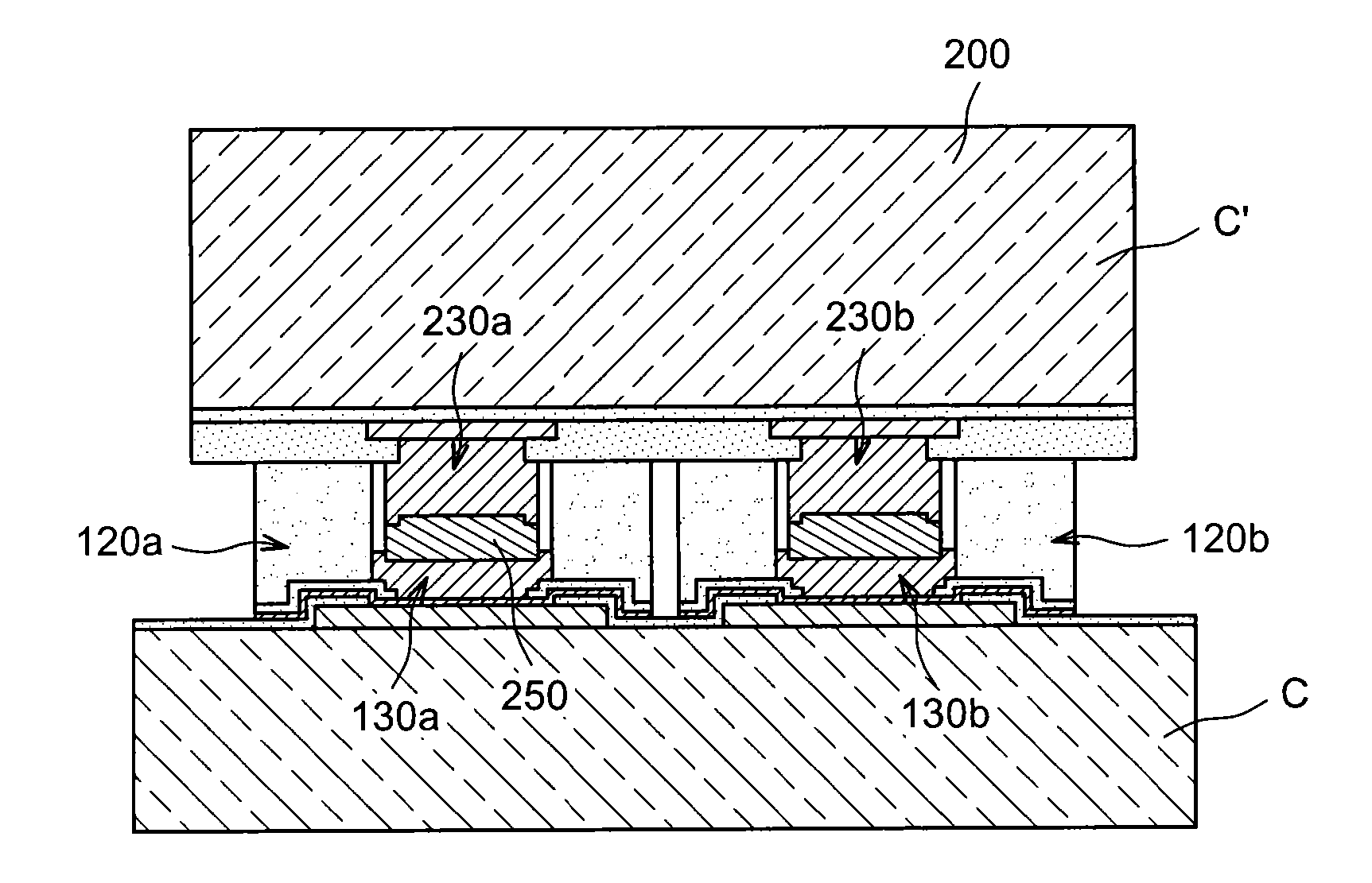
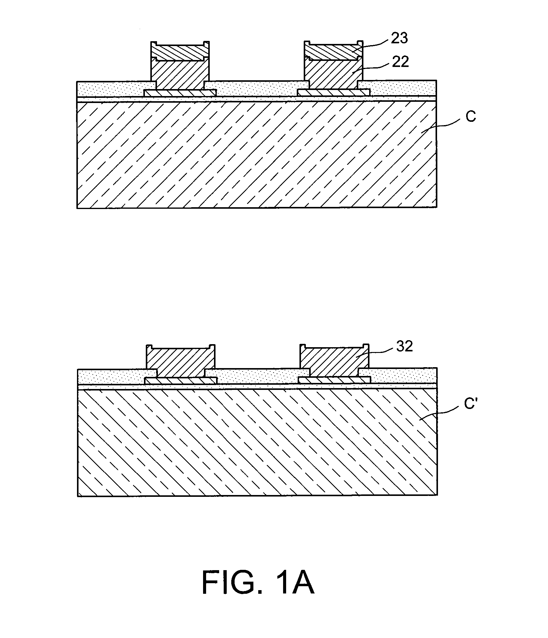
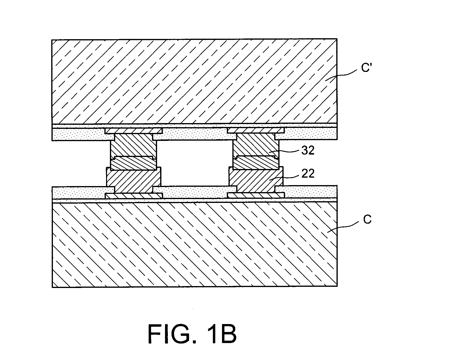
[0018]a) forming, on the first microelectronic device, a stack comprising a conductive layer applied over a top surface of a conductive pad, and a protective dielectric layer comprising at least one opening called > facing the said pad and exposing the said conductive layer;

[0019]b) forming an insulating block on a peripheral region above the top surface of the said conductive pad, the said insulating block being obtained with a cross-section forming a closed contour and comprising an opening called > located in the centre of the said insulating lock and exposing the first opening;

[0020]c) forming a conductive pillar in said at least one first opening and second opening via growth from the said conductive layer.

[0021]The height of the conductive pillar and the height of the said insulating block...


PUM


Abstract

The invention concerns the forming of a microelectronic device comprising a substrate containing at least one conductive pad, the said pad being provided with a bottom surface resting on the substrate and an upper surface opposite said bottom surface, the said upper surface of said pad having a stack applied thereto formed of a conductive layer and a protective dielectric layer comprising an opening called first opening facing said pad and exposing the said conductive layer, at least one insulating block (120a, 120b) being arranged on a peripheral region of said upper surface of said pad, the said insulating block (120a, 120b) having a cross-section forming a closed contour and comprising an opening called second opening, a conductive pillar (130a, 130b) being located in the centre of said contour in the said second opening.

Description

TECHNICAL FIELD[0001]The invention concerns the field of microelectronics and the assembly and interconnecting of microelectronic devices such as boards, substrates, chip carriers, chips, components.[0002]It provides a method to produce a structure for assembling microelectronic devices, allowing the facilitated positioning of said devices relative to one another whilst obtaining good isolation of the conductive elements allowing the interconnecting of these devices and good mechanical strength.PRIOR ART[0003]It is increasingly being sought to produce vertical stacks of chips or components.[0004]To connect together the bottom surface and top surface of a chip it is known to form connections called Through Silicon Vias (TSVs) which pass through the thickness of a substrate from which the chip is formed.[0005]To connect and assemble chips together, connecting elements in the form of micro-pillars or micro-bumps can be used. Assembly is then achieved by joining micro-pillars or micro-b...

Claims


Application Information

Patent Timeline
IPC IPC(8): H05K1/02H05K3/46H05K3/40
CPCH01L2224/13084H01L2224/81011H01L2224/16111H01L23/3171H01L21/563H01L24/03H01L24/05H01L24/11H01L24/13H01L24/16H01L24/81H01L25/0657H01L25/50H01L2224/0215H01L2224/02166H01L2224/0345H01L2224/03462H01L2224/03464H01L2224/0348H01L2224/036H01L2224/0381H01L2224/0391H01L2224/0401H01L2224/05083H01L2224/05147H01L2224/05155H01L2224/05166H01L2224/05187H01L2224/05557H01L2224/05559H01L2224/05567H01L2224/05644H01L2224/10126H01L2224/10135H01L2224/11462H01L2224/11464H01L2224/1148H01L2224/1181H01L2224/13022H01L2224/13082H01L2224/13111H01L2224/13116H01L2224/13144H01L2224/13147H01L2224/13155H01L2224/16148H01L2224/16227H01L2224/81139H01L2224/8114H01L2224/81191H01L2224/81193H01L2224/81815H01L2224/83102H01L2224/05568H01L2224/13006H01L2224/13166H01L2225/06513H01L2225/06593H01L2224/05584H01L2224/02123H01L2224/02141H01L24/73H01L24/92H01L2224/16245H01L2224/3201H01L2224/73103H01L2224/73204H01L2224/81007H01L2224/83862H01L2224/9211H01L23/49811H01L2924/00014H01L2224/16225H01L2224/73203H01L23/3192H01L2224/81024H01L2924/00015H01L2924/01047H01L2924/05442H01L2924/05042H01L2224/051H01L2924/01074H01L2224/81H01L2224/83H01L2924/00012H01L2224/05552H05K1/0296H05K3/4084H05K3/467
Inventor PARES, GABRIEL
Owner COMMISSARIAT A LENERGIE ATOMIQUE ET AUX ENERGIES ALTERNATIVES
Why Eureka
Try Eureka