Thin film type chip device and method of manufacturing the same

Inactive Publication Date: 2014-05-29
SAMSUNG ELECTRO MECHANICS CO LTD
View PDF9 Cites 16 Cited by
  • Summary
  • Abstract
  • Description
  • Claims
  • Application Information

AI Technical Summary

Benefits of technology

[0008]An object of the present invention is to provide a thin film typ

Problems solved by technology

The ferrite magnetic layer is an element involving permeability and is exposed to the outside, and thus such a generati

Method used


Image

  • Thin film type chip device and method of manufacturing the same
  • Thin film type chip device and method of manufacturing the same
  • Thin film type chip device and method of manufacturing the same

Examples


Embodiment Construction

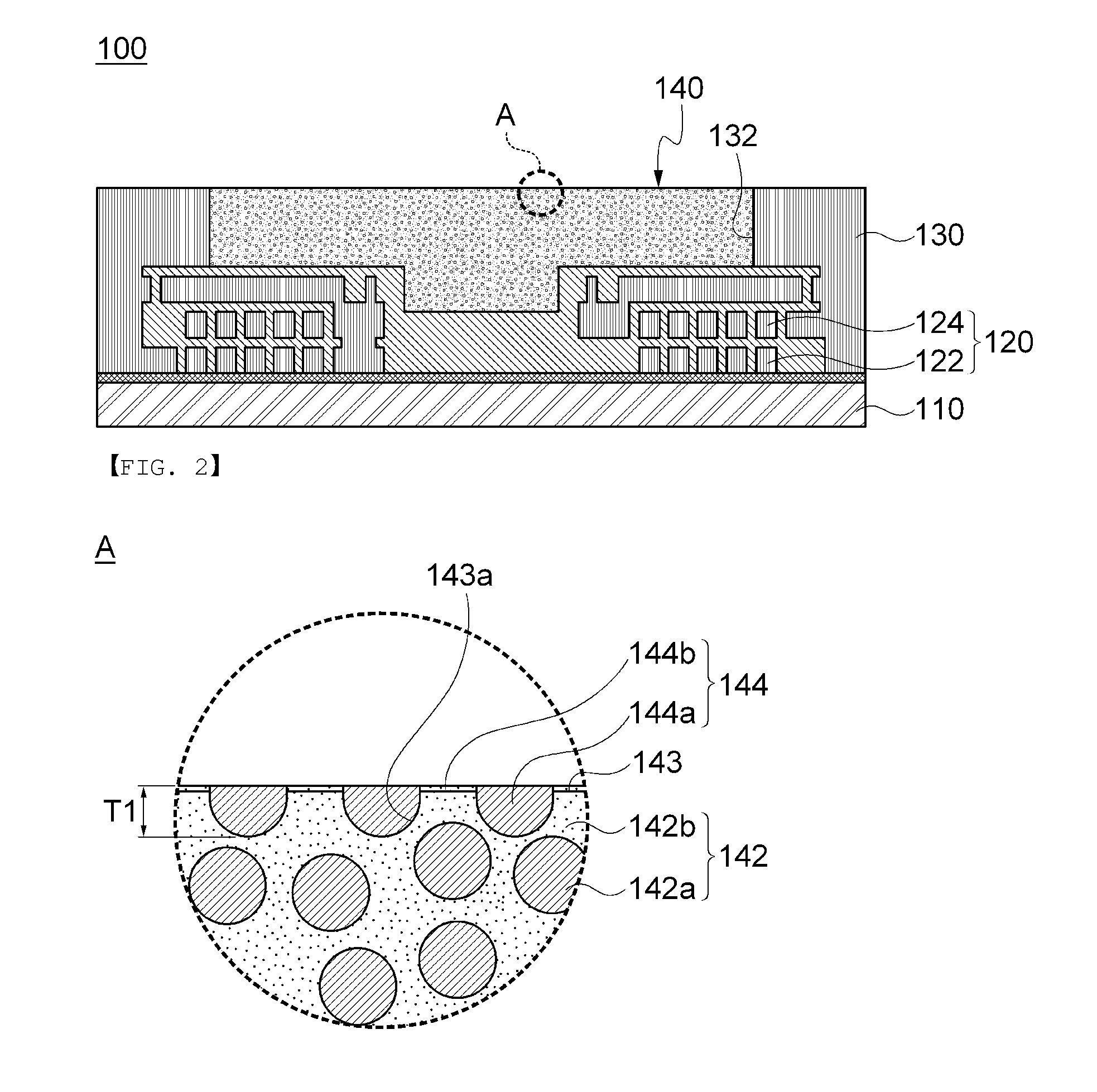
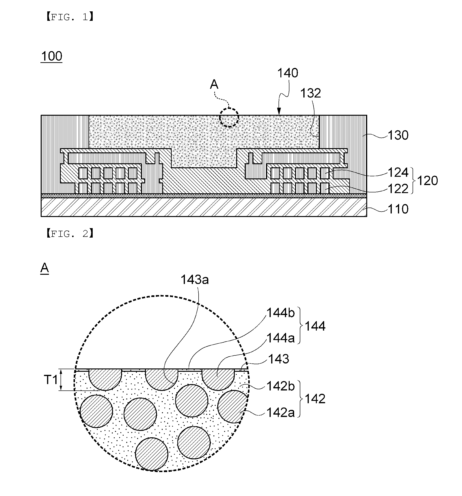
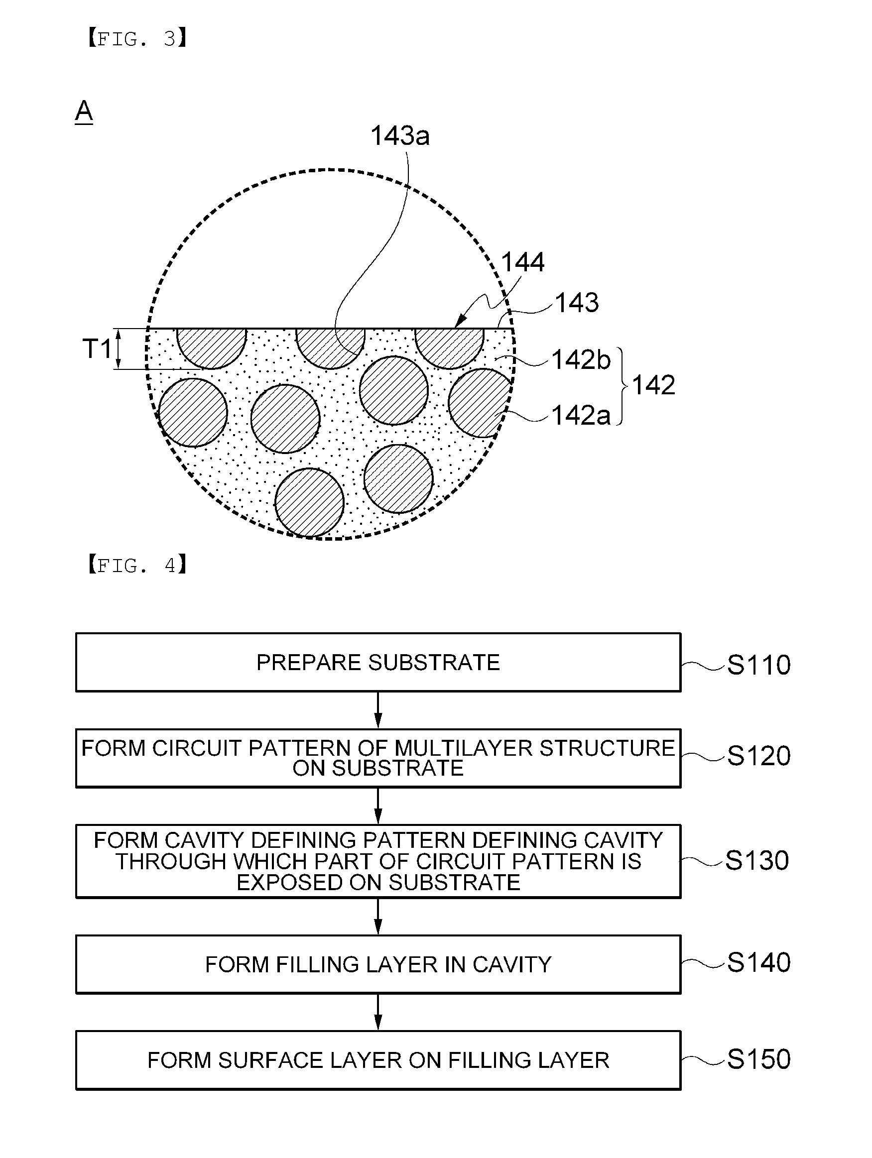
[0033]Various advantages and features of the present invention and methods accomplishing thereof will become apparent from the following description of embodiments with reference to the accompanying drawings. However, the present invention may be modified in many different forms and it should not be limited to the embodiments set forth herein. These embodiments may be provided so that this disclosure will be thorough and complete, and will fully convey the scope of the invention to those skilled in the art. Like reference numerals throughout the description denote like elements.

[0034]Terms used in the present specification are for explaining the embodiments rather than limiting the present invention. Unless explicitly described to the contrary, a singular form includes a plural form in the present specification. The word “comprise” and variations such as “comprises” or “comprising,” will be understood to imply the inclusion of stated constituents, steps, operations and / or elements b...


PUM


Abstract

Disclosed herein is a thin film type chip device including a coil pattern formed on the substrate; a cavity defining pattern defining a cavity through which a part of the coil pattern is exposed; a filling layer filled in the cavity; and a magnetic layer including a surface layer covering a surface of the filling layer.

Description

CROSS REFERENCE(S) TO RELATED APPLICATIONS[0001]This application claims the benefit under 35 U.S.C. Section 119 of Korean Patent Application Serial No. 10-2012-0133667, entitled “Thin Film Type Chip Device and Method of Manufacturing the Same” filed on Nov. 23, 2012, which is hereby incorporated by reference in its entirety into this application.BACKGROUND OF THE INVENTION[0002]1. Technical Field[0003]The present invention relates to a thin film type chip device and a method of manufacturing the thin film type chip device, and more particularly, to a thin film type chip device capable of preventing an appearance from being poor during a manufacturing process and improving permeability and impedance characteristics and a method of manufacturing the thin film type chip device.[0004]2. Description of the Related Art[0005]Recently, as electronic devices such as smart phones have been equipped with high specifications, multi functions, and small sizes, it is essential to apply chip parts...

Claims


Application Information

Patent Timeline
IPC IPC(8): H01F27/28
CPCH01F17/0013H01F2017/0066H01F41/041H05K1/165
Inventor LEE, SANG MOONBAE, JUN HEEWI, SUNG KWONKIM, YONG SUK
Owner SAMSUNG ELECTRO MECHANICS CO LTD
Why Eureka
Try Eureka