Chip varistor

a varistor and chip technology, applied in the field of varistor, can solve problems such as multi-layer varistors that can have problems, and achieve the effect of excellent clamping properties

Active Publication Date: 2014-06-19
TDK CORPARATION
View PDF6 Cites 7 Cited by
  • Summary
  • Abstract
  • Description
  • Claims
  • Application Information

AI Technical Summary

Benefits of technology

[0005]When a surge voltage like ESD (Electrostatic Discharge) is applied to the multilayer chip varistor, a property to clamp ESD (hereinafter referred to as “clamp property”) varies corresponding to the shortest dis

Problems solved by technology

However, the multilayer chip varistor c

Method used


Image

  • Chip varistor
  • Chip varistor
  • Chip varistor

Examples


Embodiment Construction

[0027]The preferred embodiments of the present invention will be described below in detail with reference to the accompanying drawings. In the description the same elements or elements with the same functionality will be denoted by the same reference signs, without redundant description.

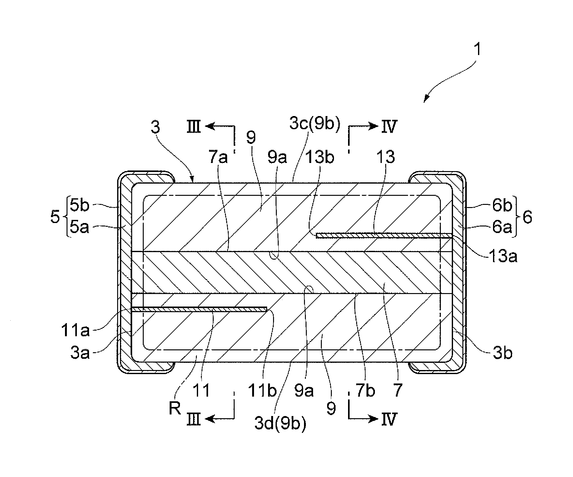
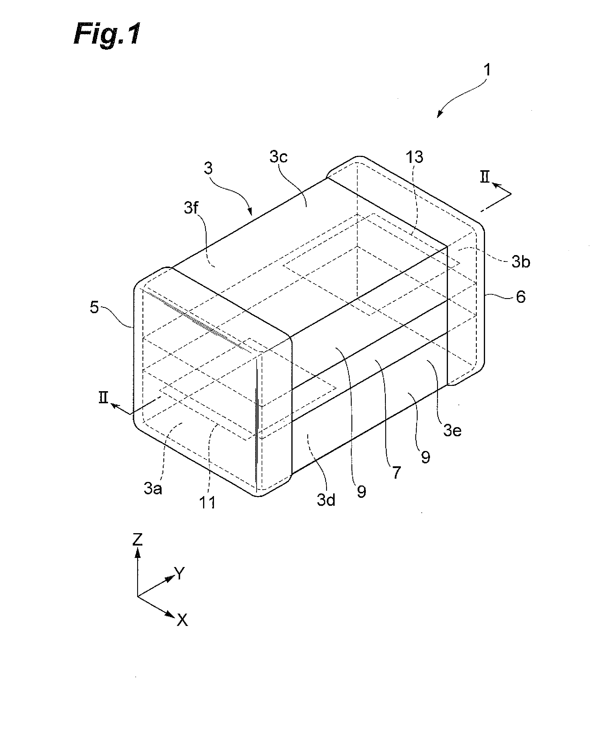
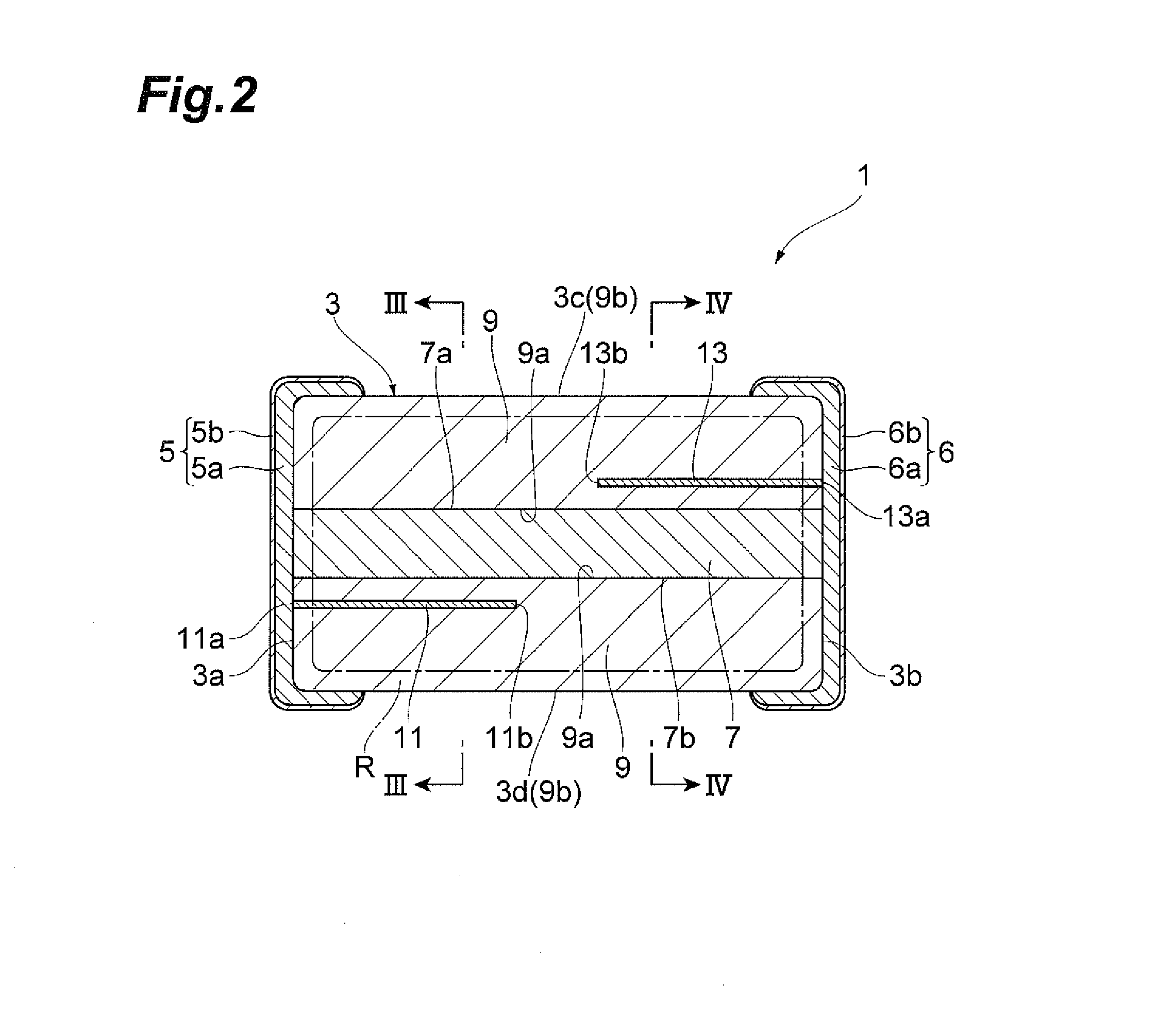
[0028]First, a configuration of chip varistor 1 according to an embodiment of the present invention will be described with reference to FIGS. 1 to 5. FIG. 1 is a perspective view showing the chip varistor according to the present embodiment. FIG. 2 is a drawing for explaining a cross-sectional configuration along the line II-II in FIG. 1. FIG. 3 is a drawing for explaining a cross-sectional configuration along the line in FIG. 2. FIG. 4 is a drawing for explaining a cross-sectional configuration along the line IV-IV in FIG. 2.

[0029]The chip varistor 1, as also shown in FIG. 1, is provided with an element body 3 of a nearly rectangular parallelepiped shape, a first terminal electrode 5, and a second t...


PUM


Abstract

An element body has first and second faces opposed to each other. A first conductor has one end exposed in a first face and the other end located in the element body. The second conductor has one end exposed in a second face and the other end located in the element body. The element body has a first element body section having the nonlinear voltage-current characteristics and a second element body section in which an electric current is more likely to flow than in the first element body section. The first element body section is located at least in part between the first conductor and the second conductor, in a direction in which the first conductor and the second conductor are separated from each other. The other end of the first conductor and the other end of the second conductor are located in the second element body section.

Description

BACKGROUND OF THE INVENTION[0001]1. Field of the Invention[0002]The present invention relates to a chip varistor.[0003]2. Related Background Art[0004]One of known chip varistors is a multilayer chip varistor provided with a varistor element body and a plurality of terminal electrodes arranged at ends of the varistor element body (e.g., cf. Japanese Patent Application Laid-Open Publication No. 2002-246207). The varistor element body has a varistor layer and a plurality of internal electrodes arranged in contact with the varistor layer so as to interpose the varistor layer between them. The plurality of terminal electrodes are connected to the respective corresponding internal electrodes. In the multilayer chip varistor, a region between the internal electrodes in the varistor layer functions as a region to exhibit the nonlinear voltage-current characteristics (hereinafter also referred to as “varistor characteristics”).SUMMARY OF THE INVENTION[0005]When a surge voltage like ESD (Elec...

Claims


Application Information

Patent Timeline
IPC IPC(8): H01C7/12
CPCH01C7/123H01C1/148H01C7/1006H01C7/18
Inventor ITAMI, TAKAHIROYOSHIDA, NAOYOSHIMORIAI, KATSUNARI
Owner TDK CORPARATION
Why Eureka
Try Eureka