

Phosphor substrate, display device, and electronic apparatus
a technology of display device and phosphor substrate, which is applied in the direction of lighting and heating apparatus, semiconductor devices for light sources, instruments, etc., can solve the problems of narrow viewing angle of liquid crystal displays, low image recognition performance when viewed from an oblique direction, and difficulty in increasing definition and siz
- Summary
- Abstract
- Description
- Claims
- Application Information
AI Technical Summary
Benefits of technology
Problems solved by technology
Method used
Image

Examples
first embodiment
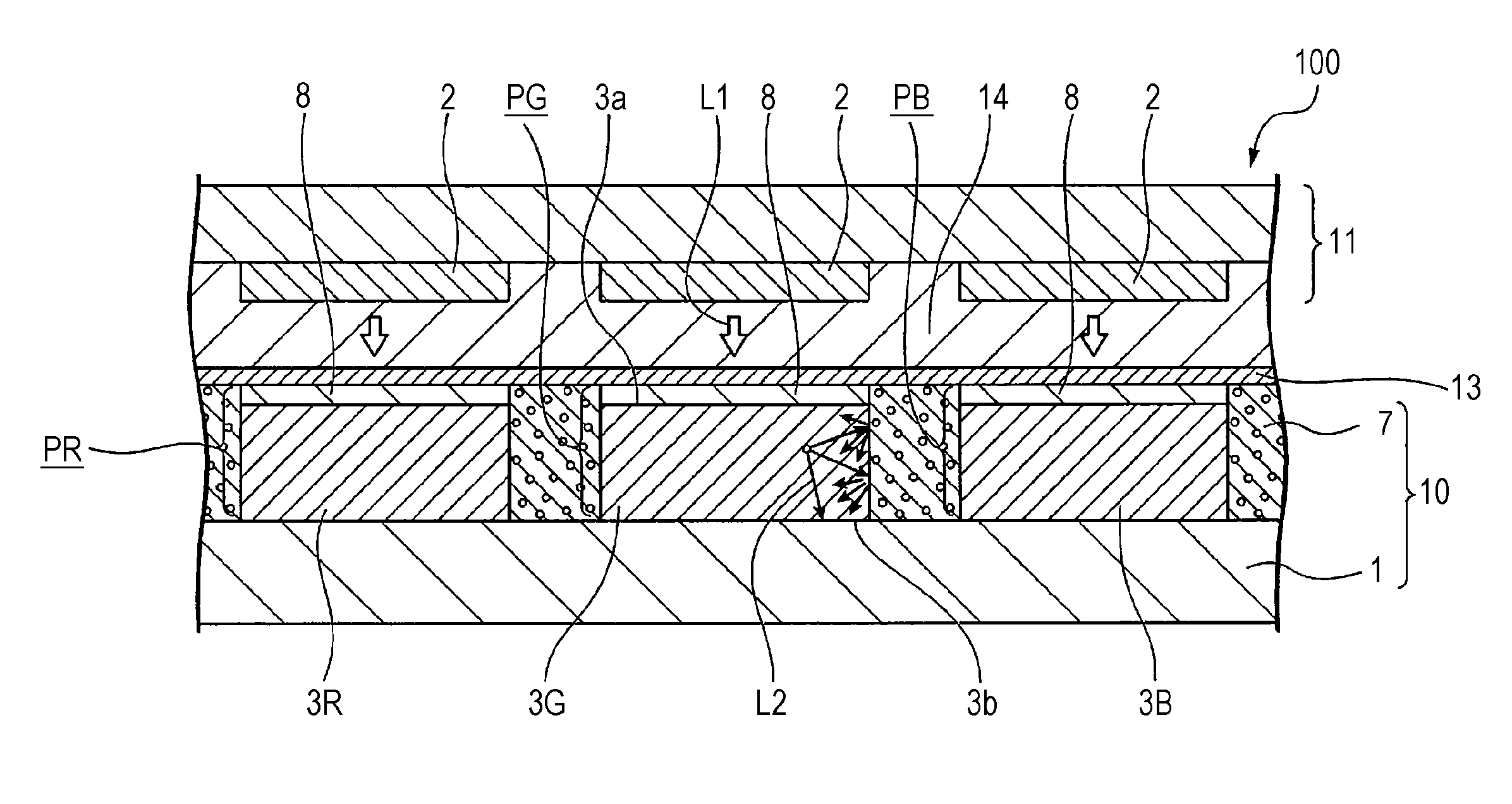
[0079]FIG. 1 is a schematic cross-sectional view of a display device 100 according to a first embodiment.
[0080]The display device 100 includes a phosphor substrate 10, a substrate 13, a light source 11, and an adhesive layer 14. The substrate 13 is provided between the phosphor substrate and the light source 11. The light source 11 includes light-emitting elements 2. Excitation light L1 to be incident on the phosphor substrate 10 is emitted from the light-emitting elements 2. The adhesive layer 14 bonds the light source 11 and the phosphor substrate 10. A common ultraviolet curable resin, a thermosetting resin, or the like may be used for the adhesive layer.
[0081]In the case where a light source is directly disposed on the phosphor substrate 10, the adhesive layer 14 may be arranged at a portion which is located at the periphery of the phosphor substrate 10 and the light source 11 and which is located between the phosphor substrate 10 and the light source 11, and a region surrounded...
second embodiment
[0204]A second embodiment of the present invention will be described below with reference to FIGS. 10 and 11.
[0205]A display device according to this embodiment has the same basic structure as the first embodiment. The structure of the partition is different from the first embodiment. Thus, in this embodiment, the description of the basic structure of the display device is omitted, and only the partition will be described.
[0206]FIG. 10 is a schematic cross-sectional view of a display device 100A according to the second embodiment.
[0207]In the first embodiment, the partition 7 includes the light-scattering particles 7a dispersed therein. In contrast, a partition 17 according to this embodiment, portions of the partition 17 (side faces of the partition 17) in contact with the phosphor layers 3R, 3G, and 3B have an uneven shape as illustrated in FIG. 10. The remaining components are the same as the first embodiment. The partition 17 is composed of a resin. The partition 17 may be compo...
third embodiment
[0212]A third embodiment of the present invention will be described below with reference to FIG. 12.
[0213]A display device 100B according to this embodiment has the same basic structure as the first embodiment, except that color filters 4 are disposed between the substrate 1 and the phosphor layers 3 and that black layers 5 and 6 are disposed on the partition 7. Thus, in this embodiment, the description of the basic structure of the display device 100B is omitted.
[0214]FIG. 12 is a schematic cross-sectional view of the display device 100B according to the third embodiment.
[0215]In the display device 100B according to this embodiment, a red color filter 4R is disposed between the substrate 1 and the red phosphor layer 3R. A green color filter 4G is disposed between the substrate 1 and the green phosphor layer 3G. A blue color filter 4B is disposed between the substrate 1 and the blue phosphor layer 3B. Thereby, it is possible to improve the chromaticity.
[0216]A first black layer 5 is...
PUM
| Property | Measurement | Unit |
|---|---|---|
| particle size | aaaaa | aaaaa |
| particle size | aaaaa | aaaaa |
| particle size | aaaaa | aaaaa |
Abstract
Description
Claims
Application Information