Touch panel

Inactive Publication Date: 2014-06-26
AVCT OPTICAL ELECTRONICS
View PDF1 Cites 3 Cited by
  • Summary
  • Abstract
  • Description
  • Claims
  • Application Information

AI Technical Summary

Benefits of technology

The patent describes a new touch panel that has a unique structure. The panel includes a row of conductive strips that are covered by a layer of insulation. This insulation layer has tiny holes in it that allow the conductive strips to touch. When a user presses on the panel, the conductive strips ensure that the user's touch is detected. The technical benefit of this touch panel is that it can provide accurate touch sensing and detection, even when the user is using a stylus or other input device.

Problems solved by technology

As a consequence, the layout design for the peripheral wires becomes extremely challenging due to a significant decrease in the border widths of display panels.
1. Narrower wire widths are used to reduce the wiring area. This approach, however, may increase the wire resistance, causing an increase in voltage drop across the wires and an interference with signal transmission. Moreover, it is difficult and cost-ineffective to produce display panels with narrower wires and this approach would easily reduce the production yield.
2. The peripheral wires are overlapped on the transparent conductive substrate, thereby reducing the wiring area. However, this approach may increase the risks of causing interference and short-circuit between the peripheral wires.

Method used


Image

  • Touch panel
  • Touch panel
  • Touch panel

Examples


Embodiment Construction

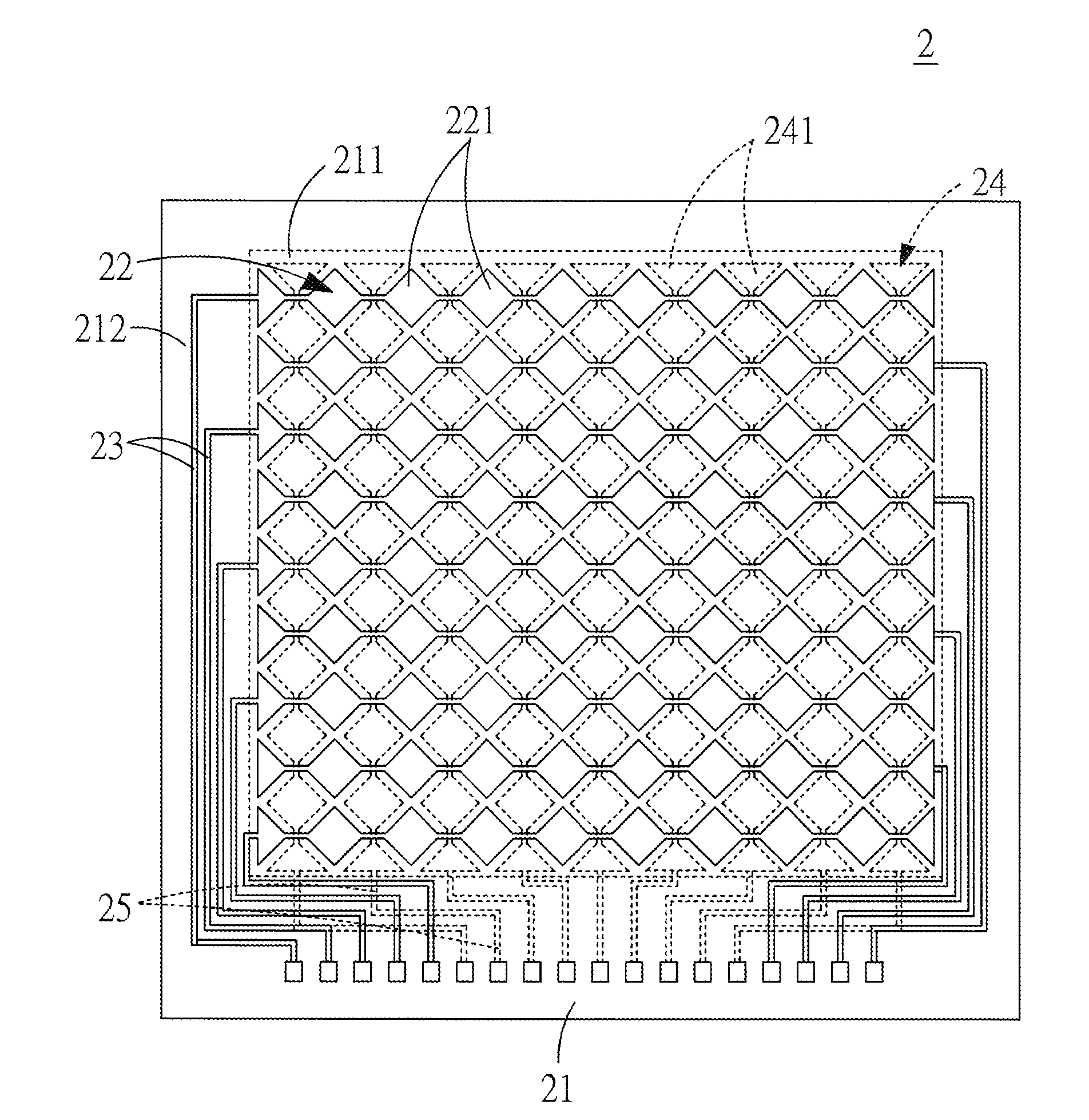
[0021]FIGS. 2(A) and (B) are schematic diagram illustrating the structure of the touch panel according to the invention, and FIG. 3 is a schematic cross-sectional diagram illustrating the touch panel according to the first preferred embodiment of the invention. As illustrated, the touch panel 2 disclosed herein comprises a first transparent substrate 21, an upper sensing pattern 22, a plurality of upper metallic wires 23, a lower sensing pattern 24, a plurality of lower metallic wires 25 and a shielding member 26.

[0022]The first transparent substrate 21 is formed with a visual region 211 and a wiring region 212 disposed around the outer periphery of the visual region 211. The first transparent substrate 21 includes an upper surface 213 and a lower surface 214 opposite to the upper surface 213.

[0023]The upper sensing pattern 22 comprises a plurality of upper sensing series 221 arranged in a first direction and resides in the visual region 211 of the first transparent substrate 21. Ac...


PUM


Abstract

The invention relates to a touch panel. The touch panel includes a first transparent substrate, and an upper sensing pattern, upper metallic wires, a lower sensing pattern, lower metallic wires and a shielding member, all disposed on the first transparent substrate. Both of the upper and lower metallic wires are disposed around an outer periphery of the visual region—the wiring region. The shielding member is arranged between to the upper metallic wires and the lower metallic wires, so that the upper metallic wires and the lower metallic wires can be arranged in a manner overlapping with each other without causing interference between the wires. The invented touch panel has a reduced wiring area, in which the wiring region is minimized.

Description

BACKGROUND OF THE INVENTION[0001]1. Field of the Invention[0002]The present invention relates to a touch panel and, more particularly, to a touch panel having a reduced wiring area, in which the wiring region of the touch panel is much narrower as compared with the conventional touch panels.[0003]2. Description of the Prior Art: In recent years, touch-sensing human-machine interface devices, such as touch panels, have been widely used in a broad variety of electrical and electronic devices, including global positioning system (GPS) devices, personal digital assistants (PDAs), cellular phones, and Hand-held PCs, in place of traditional input devices (such as a keyboard or a computer mouse). This structural innovation not only improves the communication between human and machine, but saves space by eliminating traditional input devices. As a result, the saved space can be utilized for accommodating a display panel which in turn provides the user a pleasant experience on displaying ima...

Claims


Application Information

Patent Timeline
IPC IPC(8): H05K7/02
CPCH05K9/0054
Inventor KUO, TING-CHINGLEE, JYR-DWOCHOU, SHIH-LIANGHUANG, CHUN-JUNGCHIANG, HSUEH- CHIH
Owner AVCT OPTICAL ELECTRONICS
Why Eureka
Try Eureka