Basic display driving circuit driven by conductive wire type artificial neurons

An artificial nerve and display-driven technology, applied to electrical components, biological neural network models, static indicators, etc., to achieve the effect of high effective area and less wire

Pending Publication Date: 2022-07-15
MINDU INNOVATION LAB
View PDF0 Cites 0 Cited by
  • Summary
  • Abstract
  • Description
  • Claims
  • Application Information

AI Technical Summary

Problems solved by technology

It is also very important to realize the application and development of conductive filament artificial neural devices, but the current research on the application of neuron devices is mainly used in bionic devices, intelligent sensing, image processing, and there is no report on the application in the field of drive circuit display

Method used


Image

  • Basic display driving circuit driven by conductive wire type artificial neurons
  • Basic display driving circuit driven by conductive wire type artificial neurons
  • Basic display driving circuit driven by conductive wire type artificial neurons

Examples


preparation example Construction

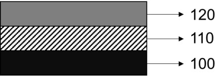
[0040] The preparation method of the basic display driving circuit driven by the conductive filament type artificial neuron specifically includes the following steps:

[0041] (1) Based on a highly doped silicon wafer or copper and platinum inert metal materials with a thickness of 100-600nm;

[0042] (2) preparing a solid dielectric layer by sputtering insulating material on the bottom metal electrode layer obtained in step (1);

[0043] (3) A top metal electrode is prepared on the obtained solid dielectric layer by a thermal evaporation process.

specific Embodiment 1

[0044] 1) A heavily doped P-type silicon wafer with a size of 1.5cm×1.5cm and a length of 100nm silicon dioxide was cut, washed with acetone, isopropanol, chloroform and distilled water (three times), and then dried with nitrogen. Afterwards, a clean silicon wafer is obtained as a substrate.

[0045] 2) Sputtering a tantalum oxide insulating layer with a thickness of 50-70 nm on the silicon wafer obtained in step 1) by sputtering under the condition that the ratio of argon gas to oxygen gas is 20:5 and the sputtering pressure is 0.5pa.

[0046] 3) A 50nm-thick top silver electrode layer with a channel length of 30 μm and a width of 1000 μm is evaporated on the silicon wafer obtained in step 2) by thermal evaporation using a special mask.

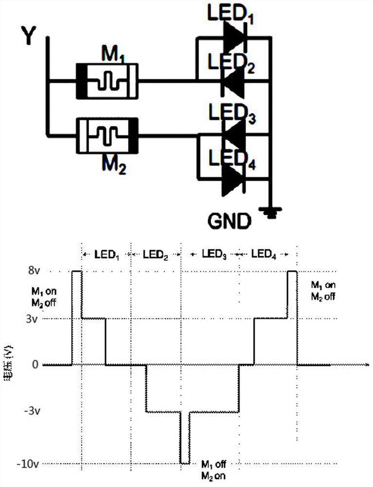
[0047] 4) One end of the first conductive wire-type artificial neural component M1 is connected to the first light-emitting device LED1 and the second light-emitting device LED2, the other end of the first conductive wire-type artificial neu...

specific Embodiment 2

[0054] (1) The cut 1.5cm×1.5cm size, heavily doped P-type silicon wafer, washed with acetone, isopropanol, chloroform and distilled water (three times), and then dried with nitrogen to obtain clean CO2 Silicon wafer as substrate.

[0055] (2) 50nm thick copper with a length of 500 μm and a width of 500 μm is sputtered as a bottom metal electrode layer on the silicon wafer obtained in step 1) by means of magnetron sputtering using a special mask.

[0056] (3) Sputtering a tantalum oxide insulating layer with a thickness of 50-70 nm on the silicon wafer obtained in step 1) by sputtering under the conditions that the ratio of argon to oxygen is 20:5 and the sputtering pressure is 0.5pa.

[0057] (4) A 50-nm-thick top silver electrode layer with a channel length of 30 μm and a width of 1000 μm is vapor-deposited on the silicon wafer obtained in step 2) by thermal evaporation using a special mask.

[0058] (5) One end of the first conductive wire-type artificial neural component M...


PUM

PropertyMeasurementUnit
thicknessaaaaaaaaaa

Abstract

The invention provides a basic display driving circuit driven by a conductive wire type artificial neuron, a conductive wire type artificial neuron component used for the display driving circuit is of a sandwich structure and sequentially comprises a bottom metal electrode layer, an insulating layer and a top metal electrode layer from bottom to top, the bottom metal electrode layer is made of an inert conductor material, and the top metal electrode layer is made of a conductive material. The insulating layer is made of an ion-migratable insulating material, and the top metal electrode layer is made of an active metal material. The light-emitting module is composed of a first light-emitting device, a second light-emitting device, a third light-emitting device and a fourth light-emitting device which are all unidirectional conductive devices. And a common grounding voltage is connected with the conductive wire type artificial nerve component and the common grounding voltage. By applying the technical scheme, 3/4 of wiring area can be reduced in circuit design, so that the purposes of short path length and high driving integration are achieved. When the neural morphological device is applied to the display driving circuit, the application field of the neural morphological device is expanded, and the conventional display driving circuit is improved.

Description

technical field [0001] The invention relates to the technical field of display driving circuits, in particular to a basic display driving circuit driven by conductive filament type artificial neurons. Background technique [0002] At present, the rapidly developing information processing era requires more dense and intelligent microprocessors, and neuromorphic engineering is an effective way to solve the overall architecture of circuits and establish ideal computing. The memory function and manipulability of memristors are similar to the synapses of neurons in living organisms, which can process and memorize signals while transmitting signals. It is also very important to realize the application and development of conductive filament artificial neural devices, but the current research on the application of neural devices is mainly used in bionic devices, intelligent sensing, image processing, and there is no report on the application in the field of driving circuit display. ...

Claims


Application Information

Patent Timeline
Patent Type & Authority Applications(China)
IPC IPC(8): G09G3/32G06N3/063H05B45/30
CPCG09G3/32G06N3/063H05B45/30
Inventor 陈惠鹏周正贤张翔鸿凌永杰陈耿旭杨倩郭太良
Owner MINDU INNOVATION LAB
Why Eureka
Try Eureka