Integrated circuit

Inactive Publication Date: 2005-06-21
RICOH ELECTRONIC DEVICES CO LTD
View PDF8 Cites 0 Cited by
  • Summary
  • Abstract
  • Description
  • Claims
  • Application Information

AI Technical Summary

Benefits of technology

[0014]According to this present invention, the wirings routed over the semiconductor chip can be made in accordance with the number of bits of the signal lines alone even at maximum, and the wiring area as a whole can be reduced more significantly than ever before.
[0015]Additionally, according to other characteristics of the present invention, decoding circuits are arranged individually corresponding to each functional block, and wirings of the signal lines, which are small in number, to each decoding circuit is possible. Thus, the area of wirings routed over the semiconductor chip can be sufficiently reduced.
[0016]Moreover, according to other characteristics of the present invention, it is possible that the wirings from the decoding circuits to the functional blocks, which are large in number, can be made as short as possible, and the wiring area of the entire semiconductor chip can be further reduced.

Problems solved by technology

Thus, this causes a problem in that an extremely large number of wirings are routed over the semiconductor chip 100, and the chip area increased in accordance with that amount.
Also, since many wirings are routed over the semiconductor chip 100, noise is caused on the adjacent wirings when a high-speed signal is transmitted.
This is also a problem where so-called “crosstalknoise is caused in many places.
Thus, there has been an additional problem where designing a suitable chip layout is very difficult and the efficiency of the development of integrated circuits declined.

Method used


Image

  • Integrated circuit
  • Integrated circuit
  • Integrated circuit

Examples


Embodiment Construction

[0019]One embodiment of the present invention is hereinafter explained with reference to the drawings.

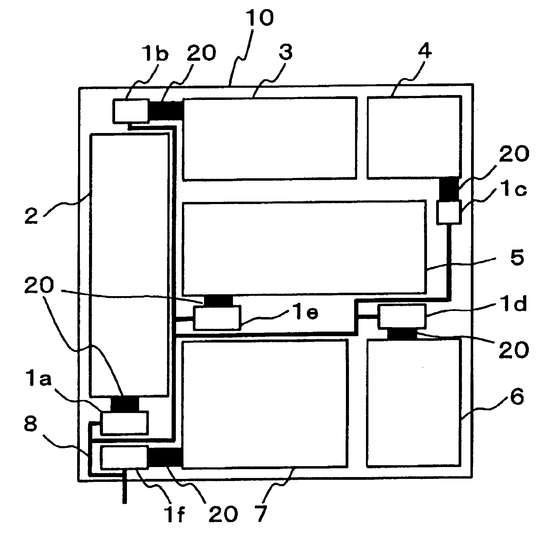
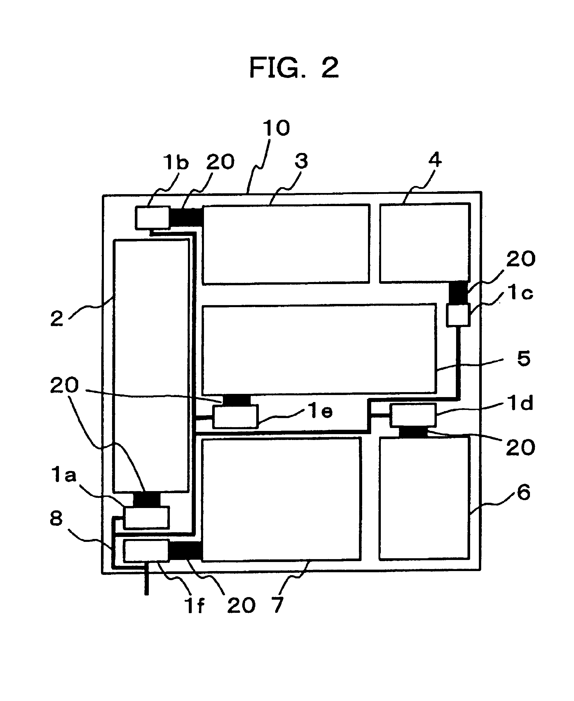
[0020]FIG. 2 is a schematic diagram showing an example of the structure of a semiconductor chip 10 for which the integrated circuits of the present invention are implemented. The semiconductor chip 10 of this embodiment integrates a plurality of decoding circuits 1a to 1f which are comprised by the serial interface circuits and a plurality of circuit blocks 2 to 7.

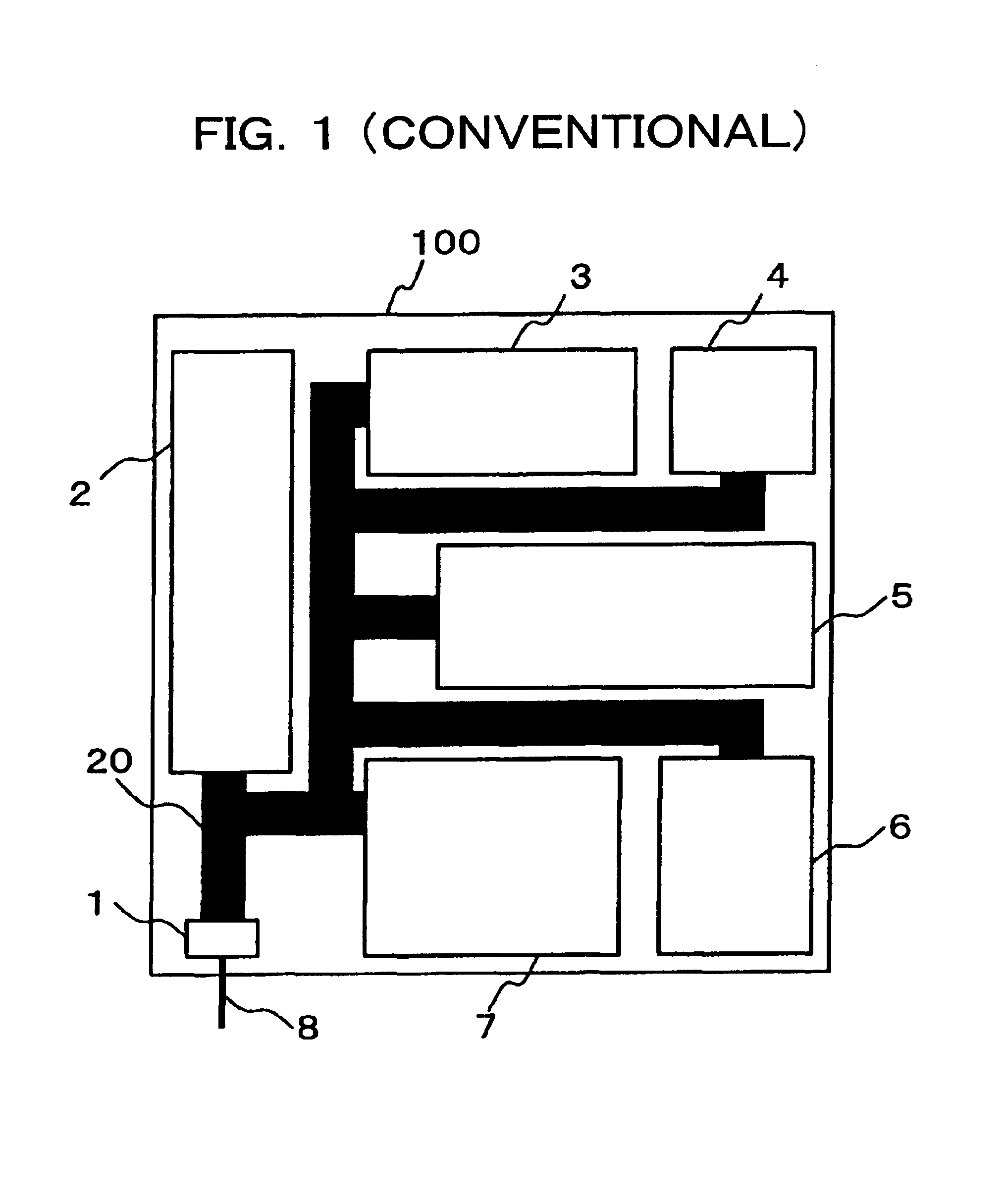
[0021]A plurality of circuit blocks 2 to 7 are a collection of functional blocks used to realize different functions. Through the mutual operations of such functional blocks, targeted data processing is executed. The sizes of such circuit blocks 2 to 7 are the same as the conventional examples shown in FIG. 1.

[0022]In this embodiment, the number of decoding circuits 1a to 1f that are integrated is the same as the number of the circuit blocks 2 to 7. And such plurality of decoding circuits 1a to 1f are arranged near a plura...


PUM


Abstract

A plurality of decoding circuits 1a to 1f are arranged near a plurality of circuit blocks 2 to 7, which are arranged on the semiconductor chip 10 in a scattered manner, and the signal lines 8 prior to decoding, including the address lines and the data lines, are wired to each decoding circuit 1a to 1f. Through these wirings, the number of wirings routed over on the semiconductor chip 10 can be made in accordance with the number of bits of the signal lines 8 alone. So, compared with the past where the signal lines 20, which were great in number after decoding, were routed over to each circuit block 2 to 7, the wiring area as a whole can be greatly reduced. This can lead to miniaturization of chip size, reduction of crosstalk noise, and facilitation of layout.

Description

CROSS REFERENCE TO RELATED APPLICATIONS[0001]This Application is a Continuation of application PCT / JP02 / 06971 filed on Jul. 10, 2002. PCT / JP02 / 06971 claims priority for application 2001-220875 filed on Jul. 23, 2001 in Japan.FIELD OF THE INVENTION[0002]The present invention relates to an integrated circuit. In particular, the present invention is suitable for use for integrated circuits for which a plurality of functional blocks are integrated within a single semiconductor chip.BACKGROUND OF THE INVENTION[0003]In recent years, integration of semiconductor chips has progressed, and circuit blocks that realize many more functions have been integrated into a single chip. When a plurality of circuit blocks are integrated within a single chip, wirings used to exchange signals are connected to each circuit block.[0004]When digital data or a digital control signal is supplied to each circuit block within a semiconductor chip, wirings to each circuit block are required, in accordance with t...

Claims


Application Information

Patent Timeline
IPC IPC(8): G11C7/02H01L31/0264H01L31/0336H01L23/522H01L27/02
CPCH01L27/0203H01L23/5222H01L2924/0002H01L2924/00
Inventor KARASUDANI, MUNEHIRO
Owner RICOH ELECTRONIC DEVICES CO LTD
Why Eureka
Try Eureka