
Method and system for in-line real-time calculation of thicknesses of semiconductor layers of a photovoltaic device

a photovoltaic device and semiconductor layer technology, applied in the field of photovoltaic devices, can solve the problems of not having a method of accurately measuring the thickness of the semiconductor layer as the device, slowing down the manufacturing line, and adding additional costs to the final cost of the photovoltaic devi

Inactive Publication Date: 2014-07-03
FIRST SOLAR INC (US)
View PDF10 Cites 3 Cited by
  • Summary
  • Abstract
  • Description
  • Claims
  • Application Information

AI Technical Summary

Benefits of technology

The patent text describes a system and method for calculating the thicknesses of semiconductor layers in photovoltaic devices in real-time, as they are being formed. The current methods for measuring the thicknesses of these layers involve stopping the manufacturing process and using microscopic cross-sectional measurements, which is time-consuming and costly. The patent proposes a non-destructive method for measuring the semiconductor layer thicknesses using LED sensors and beta backscattering. This method assumes that the thickness and optical properties of the TCO layer or stack are always the same, but this may introduce error into the thickness measurement due to manufacturing variations. The patent aims to improve the accuracy of the thickness measurements of the semiconductor layers in photovoltaic devices.

Problems solved by technology

Presently, there is not a method for accurately measuring the thicknesses of the semiconductor layers as the devices are being formed.
Doing so, however, may slow down the manufacturing line as layer deposition may have to be stopped awaiting the results of the measurements to determine whether adjustments to the deposition equipment are needed.
Further, since the device is destroyed in order to take the measurements, additional costs may be added to the final cost of the photovoltaic devices.
However, inevitable manufacturing variations in the thickness and optical properties of the TCO stack, e.g., from device to device, will cause variations in the reflection caused by the TCO stack.
Thus, the assumption that the thickness and optical properties of the TCO layer or stack is always the same, introduces error into using this method for calculating the semiconductor layer thickness.
Further, overspray of the CdS vapor from the semiconductor window deposition process onto the backside of the substrate and accumulation of the CdS vapor on the sensor windows over time can both also affect the measurements taken by the sensors.

Method used


Image

  • Method and system for in-line real-time calculation of thicknesses of semiconductor layers of a photovoltaic device
  • Method and system for in-line real-time calculation of thicknesses of semiconductor layers of a photovoltaic device
  • Method and system for in-line real-time calculation of thicknesses of semiconductor layers of a photovoltaic device

Examples


Embodiment Construction

[0018]In the following detailed description, reference is made to the accompanying drawings which form a part hereof, and in which is shown by way of illustration specific embodiments that may be practiced. These embodiments are described in sufficient detail to enable those skilled in the art to make and use them, and it is to be understood that structural, logical, or procedural changes may be made to the specific embodiments disclosed without departing from the spirit and scope of the invention.

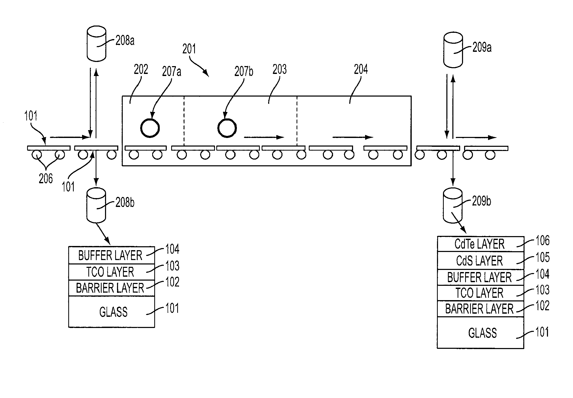
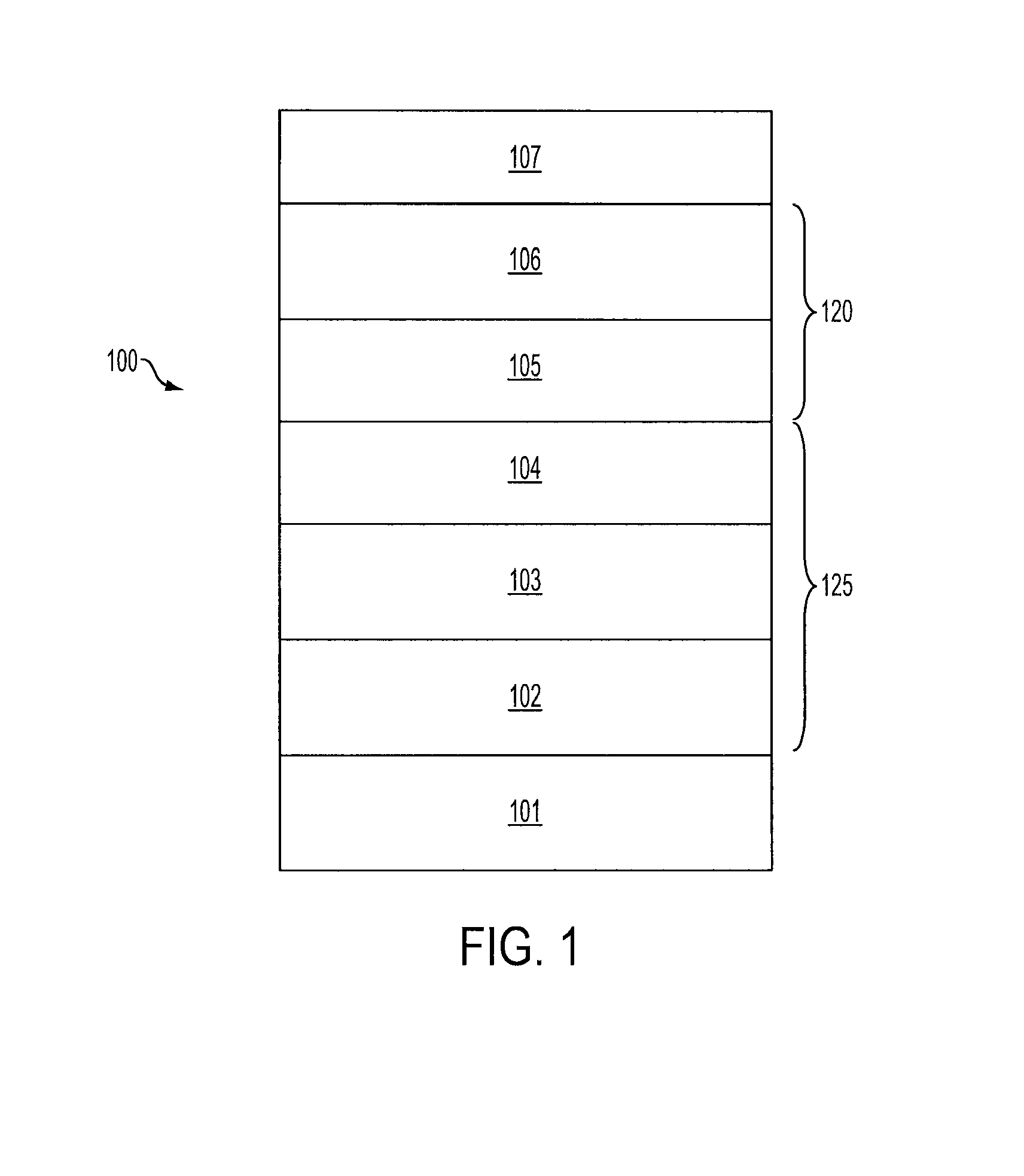
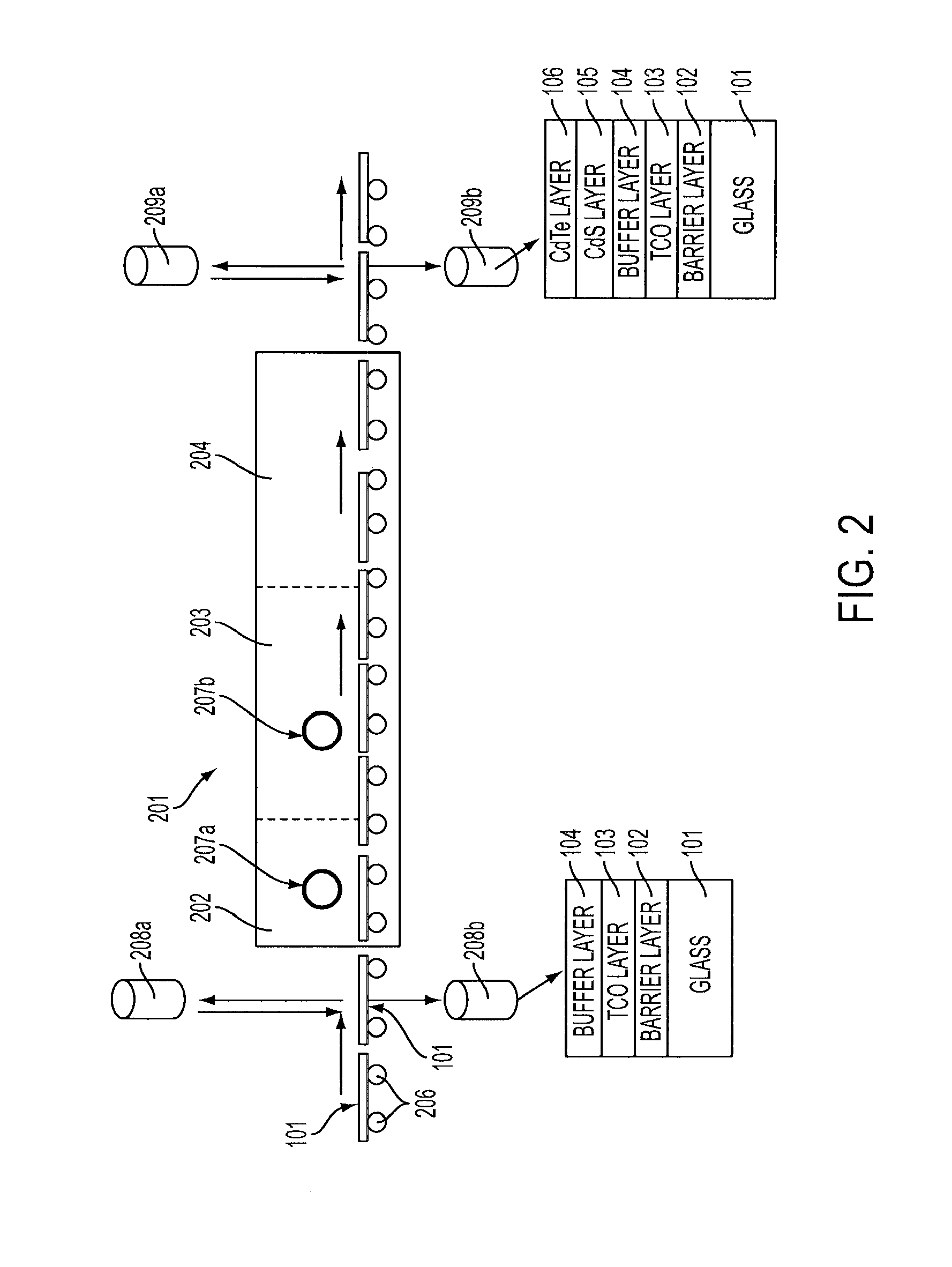
[0019]Referring to the figures, FIG. 1 shows one example of a general structure of a photovoltaic (PV) device 100. The photovoltaic device 100 includes a TCO stack 125 formed over substrate 101. The TCO stack 125 may include a barrier layer 102, a TCO layer 103 and a buffer layer 104. The photovoltaic device also includes semiconductor layer(s) 120 which include a semiconductor window layer 105 formed adjacent a semiconductor absorber layer 106. A back contact (electrode) 107 can be formed...


PUM


Abstract

A method and system for real-time, in-line measurements of thicknesses of semiconductor layers of photovoltaic devices is provided. The method and system include taking ex-situ optical data measurements after deposition of the semiconductor layers. The measurements are then used to calculate the thicknesses of the layers in real-time using optical modeling software.

Description

CROSS-REFERENCE TO RELATED APPLICATION[0001]This application claims priority to U.S. Provisional Application No. 61 / 746,379, filed Dec. 27, 2012, which is hereby fully incorporated by reference.FIELD OF THE INVENTION[0002]The disclosed embodiments relate generally to photovoltaic devices, and more particularly, to a system and method of calculating, in real-time, thicknesses of the semiconductor layers of photovoltaic devices.BACKGROUND OF THE INVENTION[0003]A variety of thin film photovoltaic devices, such as cells and modules, are known. During fabrication of such devices, layers of semiconductor material are commonly formed on a transparent conductive oxide (TCO) stack, which is used as a contact for the devices. The semiconductor layers commonly include one layer serving as a window layer and a second layer serving as an absorber layer. The absorber layer is often made of a p-type semiconductor material and the window layer of an n-type semiconductor material and the point at wh...

Claims


Application Information

Patent Timeline
IPC IPC(8): G01B11/06
CPCG01B11/0625G01B11/0616H02S50/10Y02E10/50
Inventor BULLER, BENYAMINHWANG, DAVIDMILLIRON, BENJAMINROBERTS, DALESHAO, RUIZHAO, ZHIBO
Owner FIRST SOLAR INC (US)
Learn More