Memory device and a memory module having the same

Inactive Publication Date: 2014-07-03
SAMSUNG ELECTRONICS CO LTD
View PDF6 Cites 9 Cited by
  • Summary
  • Abstract
  • Description
  • Claims
  • Application Information

AI Technical Summary

Benefits of technology

[0006]Exemplary embodiments of the inventive concept provide a memory device capable of reduc

Problems solved by technology

However, the increase in the operating frequency of the data bus is physically limited by a capac

Method used


Image

  • Memory device and a memory module having the same
  • Memory device and a memory module having the same
  • Memory device and a memory module having the same

Examples


Example

[0040]Hereinafter, exemplary embodiments of the inventive concept will be described in detail with reference to the accompanying drawings. However, the inventive concept may be embodied in various different forms, and should not be construed as being limited to the illustrated embodiments.

[0041]It will be understood that when an element or layer is referred to as being “connected to,” or “coupled to” another element or layer, it can be directly connected or coupled to the other element or layer, or intervening elements or layers may be present.

[0042]As used herein, the singular forms “a,”“an,” and “the” are intended to include the plural forms as well, unless the context clearly indicates otherwise.

[0043]Like reference numerals may refer to like elements throughout the specification and drawings.

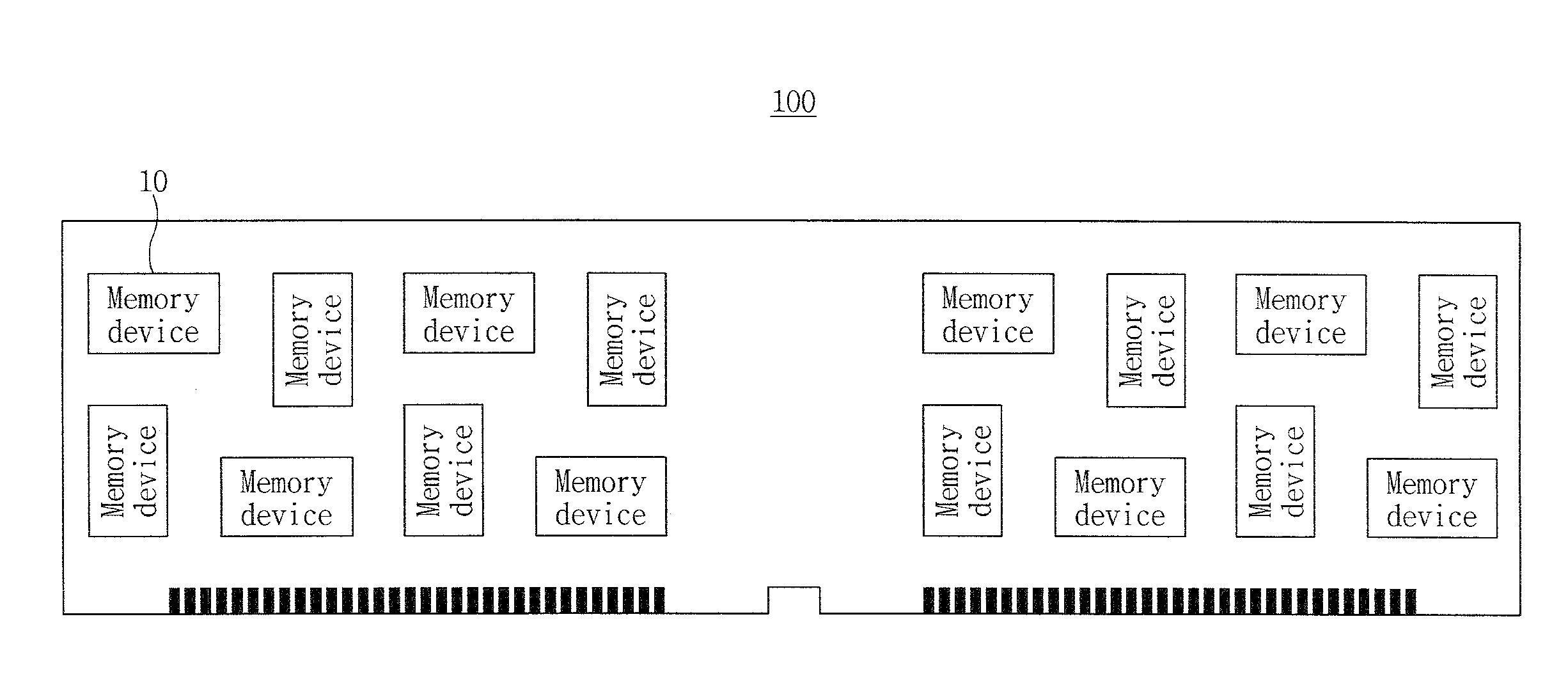
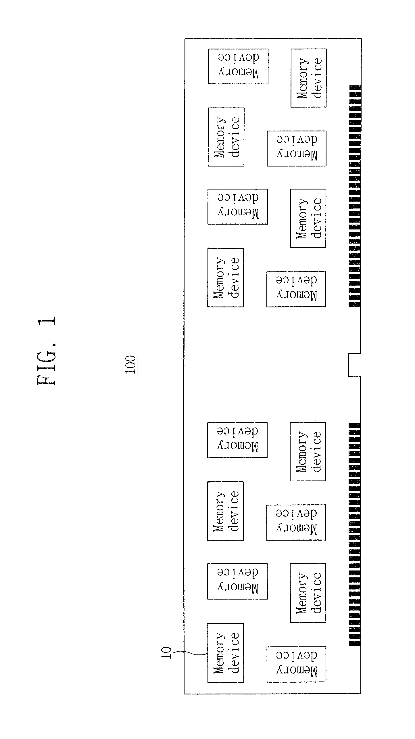
[0044]FIG. 1 is a block diagram of a memory module 100 in accordance with an exemplary embodiment of the inventive concept.

[0045]Referring to FIG. 1, the memory module 100 may include sixtee...


PUM


Abstract

A memory device is provided. The memory device includes a plurality of memory chips, and a buffer chip connected to the plurality of memory chips. The plurality of memory chips and the buffer chip are disposed in a stack. A first input/output (IO) port of the buffer chip is connected in series to an external device, and a second IO port of the buffer chip is connected in parallel to IO ports of each of the plurality of memory chips.

Description

CROSS-REFERENCE TO RELATED APPLICATIONS[0001]This application claims priority under 35 U.S.C. §120 to U.S. Patent Application No. 61 / 746,690 filed on Dec. 28, 2012, and claims priority under 35 U.S.C. §119 to Korean Patent Application No. 10-2013-0026948 filed on Mar. 13, 2013, the disclosures of which are incorporated by reference herein in their entireties.BACKGROUND[0002]1. Technical Field[0003]The inventive concept relates to a memory device and a memory module including the same, and more particularly, to a memory device embodied as a multi-chip package on which a plurality of dynamic random access memories (DRAMs) and a buffer chip are stacked, and a memory module including the same.[0004]2. Discussion of the Related Art[0005]An increase in the capacity or operating frequency of a memory module may improve the performance of a memory system. For example, an increase in the operating frequency of a data bus connected to the memory module may improve the performance of the memor...

Claims


Application Information

Patent Timeline
IPC IPC(8): G11C7/10
CPCG11C7/1072G11C5/04G11C7/10G11C7/1057G11C7/1084H01L2224/32145H01L2224/48091H01L2224/48227H01L2224/73265H01L2924/15311H01L24/73H01L2924/00012
Inventor CHOI, JUNG-HWAN
Owner SAMSUNG ELECTRONICS CO LTD
Why Eureka
Try Eureka