Touch panel substrate and electro-optical device

a technology of electro-optical devices and substrates, applied in the field of touch panel substrates, can solve the problems of increasing the noise that is received by the touch panel, the inability to correct the position of contact, and the reduction of the signal-to-noise ratio, so as to reduce the cr time constant, and reduce the resistance of the position detecting electrod

Active Publication Date: 2014-07-17
SHARP KK
View PDF3 Cites 76 Cited by
  • Summary
  • Abstract
  • Description
  • Claims
  • Application Information

AI Technical Summary

Benefits of technology

[0042]Moreover, it is possible to reduce the resistance of the position detecting electrode as described above, and this makes it possible to reduce the CR time constant.
[0046]As above described, according to the touch panel substrate and the electro-optic device of the present invention, the position detecting electrode, which is sandwiched between the insulating substrate and the electro-optic element driving electrode, at least has the first electrodes that are electrically connected to the grid of metal wires via the insulating layer. With the configuration, the resistance of the position detecting electrode can be reduced while the optical transmittance and the area of the transparent region are ensured. Therefore, mounting the touch panel substrate in a display panel makes it possible to reduce the resistance of the position detecting electrode while ensuring the aperture ratio of the display panel.
[0048]Therefore, according to the configuration, it is possible to provide (i) the touch panel substrate that is high in position detection performance, capable of carrying out a stable position detecting operation, and used in an in-cell touch panel and (ii) the electro-optic device which includes such a touch panel substrate.

Problems solved by technology

However, the capacitive touch panel, which detects the position of contact by detecting a change in capacitance, might be incapable of correct detection of the position of contact due to a change in line of electric force that is caused by extrinsic noise received by the touch panel.
However, the provision of a touch panel on the outer side of a display panel undesirably causes emission noise to be generated from the display panel when a touch panel operation is carried out while a display is being carried out, so that there is an increase in the amount of noise that is received by the touch panel.
For this reason, the provision of a touch panel on the outer side of a display panel might cause a reduction in SN ratio (signal-to-noise ratio), with the result that the touch panel deteriorates in detection performance and therefore wrongly detects the position of contact.
Further, the provision of a touch panel on the outer side of a display panel undesirably causes the resulting device to increase in thickness and weight due to the stacking of the touch panel on the display panel.
Moreover, the provision of a touch panel on the outer side of a display panel causes outside light to be reflected not only on a surface of the touch panel but also at the interface between the touch panel and the display panel, so that contrast and viewability are adversely affected.
Further, the provision of a touch panel on the outer side of a display panel causes viewability to deteriorate due to the touch panel per se.

Method used


Image

  • Touch panel substrate and electro-optical device
  • Touch panel substrate and electro-optical device
  • Touch panel substrate and electro-optical device

Examples


embodiment 1

[0116]An embodiment of the present invention is described below with reference to FIG. 1 through (a) through (e) of FIG. 19.

[0117]The present embodiment is described below by taking a liquid crystal display device as an example of an electro-optic device including an in-cell touch panel. However, the present embodiment is not to be limited to such an example.

[0118]

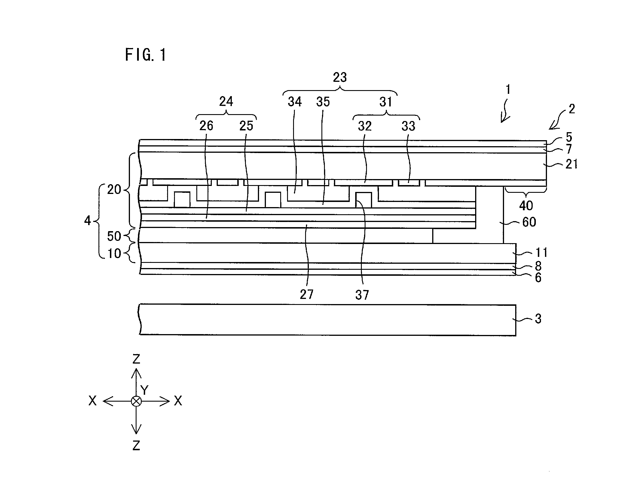
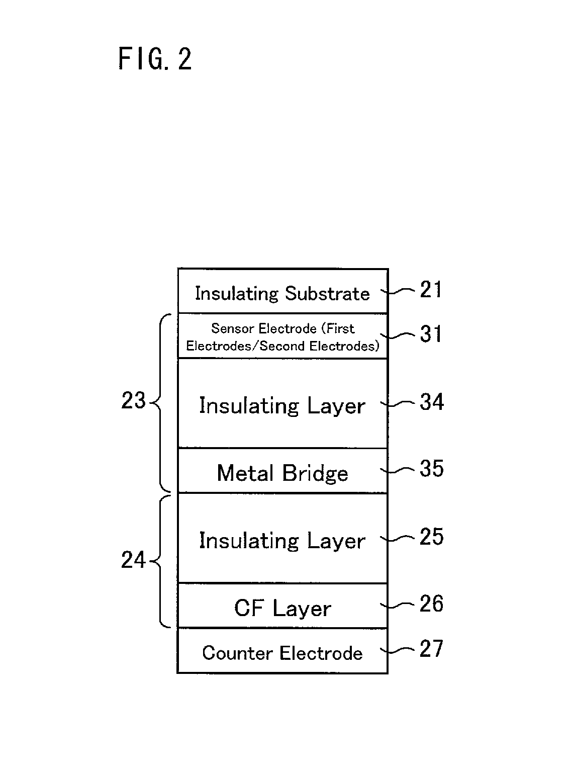
[0119]FIG. 1 is a cross-sectional view schematically showing a configuration of a main part of a liquid crystal display device according to the present embodiment.

[0120]As shown in FIG. 1, a liquid crystal display device 1 (display device) according to the present embodiment includes a liquid crystal panel 2 (display panel), a backlight 3 (illuminating device) for irradiating the liquid crystal panel 2 with light, and a driving circuit etc. (not illustrated).

[0121]Since the backlight 3 is configured in the same manner as has conventionally been configured, the following omits to describe a configuration of the backlight 3....

embodiment 2

[0313]Another embodiment of the present invention is described below with reference to FIGS. 20 through 22. For convenience of explanation, constituent elements of the present embodiment that are identical in function to their respective corresponding constituent elements used in Embodiment 1 are each assigned an identical reference sign, and as such, are not described here.

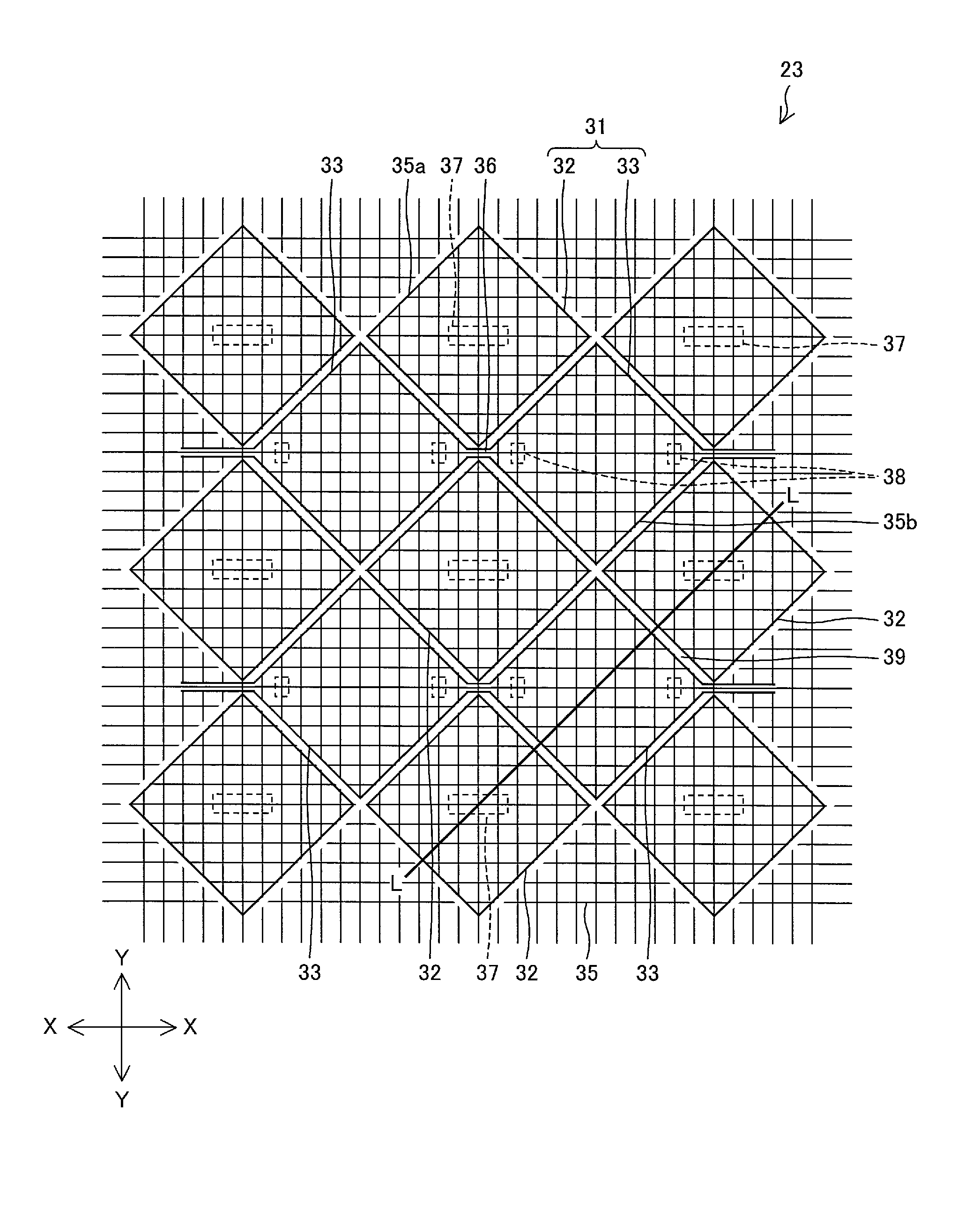
[0314]FIG. 20 is a plan view showing a configuration of a main part of a touch panel layer 23 of a substrate 20 according to the present embodiment. (a) of FIG. 21 is a diagram showing a cross-section of the substrate 20 as taken along the line Y2-Y2 across the touch panel layer 23 shown in FIG. 20. (b) of FIG. 21 is a diagram showing a cross-section of the substrate 20 as taken along the line X3-X3 across the touch panel layer 23 shown in FIG. 20.

[0315]Further, FIG. 22 is a plan view schematically showing a configuration of a metal bridge 35 shown in FIG. 20.

[0316]Embodiment 1 is configured such that in a case w...

embodiment 3

[0337]Still another embodiment of the present invention is described below with reference to FIGS. 23 through 28. For convenience of explanation, constituent elements of the present embodiment that are identical in function to their respective corresponding constituent elements used in Embodiment 1 are each assigned an identical reference sign, and as such, are not described here.

[0338]FIG. 23 is a plan view showing a configuration of a main part of a touch panel layer 23 of a substrate 20 according to the present embodiment. FIG. 24 is a diagram showing a cross-section of the substrate 20 as taken along the line X4-X4 across the touch panel layer 23 shown in FIG. 23.

[0339]Further, FIG. 25 is a plan view schematically showing a configuration of a metal bridge 35 shown in FIG. 23.

[0340]Embodiment 2 is configured such that by forming two disconnecting lines 39 across the metal bridge 35 between (i) each of the electrodes 32, which are arranged along the Y-axis, and (ii) an electrode 3...


PUM


Abstract

A sensor electrode (31) provided between an insulating substrate (21) and a counter electrode (27) is electrically connected to a grid-shaped metal bridge (35) via an insulating layer.

Description

TECHNICAL FIELD[0001]The present invention relates to a touch panel substrate that is used in an in-cell touch panel and an electro-optic device including such a touch panel substrate.BACKGROUND ART[0002]In recent years, there has been widespread use of electro-optic devices, such as display devices, each having an integration of display section and an input section for reduction in size of the devices. In particular, in the case of portable terminals such as mobile phones, PDAs (personal digital assistants), and laptop personal computers, there has been widespread use of display devices each including a touch panel that is capable of detecting the position of contact between a display surface and a finger or stylus brought into contact with the display surface.[0003]There have conventionally been known various types of touch panel such as so-called resistive (pressure-sensitive) touch panels and capacitive touch panels. Among them, so-called capacitive touch panels have been in wid...

Claims


Application Information

Patent Timeline
Patent Type & Authority Applications(United States)
IPC IPC(8): G06F3/044
CPCG06F3/044G02F1/13338G06F3/0412G06F3/0443G06F3/0446
Inventor SUGITA, YASUHIROKIDA, KAZUTOSHIYAMAGISHI, SHINJIYASHIRO, YUHJIOGAWA, HIROYUKI
Owner SHARP KK
Why Eureka
Try Eureka