Vortex magnetic random access memory

a random access memory and magnetic random access technology, applied in the field of mram cell structure, can solve the problems of inability to control the switching field, the magnetic state of a half-selected cell may be undetected, and the switching field is highly variable, so as to reduce the exchange coupling constant

Inactive Publication Date: 2006-02-02
HEADWAY TECH INC
View PDF7 Cites 29 Cited by
  • Summary
  • Abstract
  • Description
  • Claims
  • Application Information

AI Technical Summary

Benefits of technology

[0020] For the reference layer, the magnetization vortex is generated in the following manner. The vortex is fixed (pinned) by applying a temperature above a certain critical temperature so that the AFM layer is in a paramagnetic phase and then cooling down to set the vortex pinning direction. In the case of a PtMn AFM layer, the MTJ is patterned to provide the intended elliptical shape without annealing the PtMn to its anti-ferromagnetic phase. At the annealing temperature of PtMn, a vortex state is induced in the reference layer and the PtMn layer is changed into an AFM phase. The vortex state is more easily induced in the free layer and reference layer by adding a dopant comprised of one or more of C, N, B, Ta, Pt, Zr, Nb, or Hf which reduces the exchange coupling constant.

Problems solved by technology

Due to variations in MTJ size and shape that affect the switching field of a free layer, a magnetic state in a half-selected cell may be undesirably altered when writing to a selected cell.
A problem with these designs is that coercivity is highly dependent on shape, aspect ratio, and MTJ cell size and is therefore very sensitive to cell shape and edge shape which are subject to variations because of cell patterning processes.
As a result, MTJ cell differences make the switching field highly variable and difficult to control.
To prevent thermal agitation of half-selected cells, greater magnetic anisotropy is required which in turn demands a very high write current that renders MRAM non-competitive against other existing technologies because of high current and power consumption.

Method used


Image

  • Vortex magnetic random access memory
  • Vortex magnetic random access memory
  • Vortex magnetic random access memory

Examples


Embodiment Construction

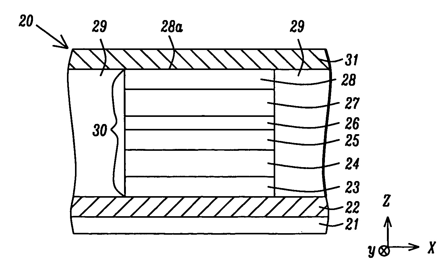
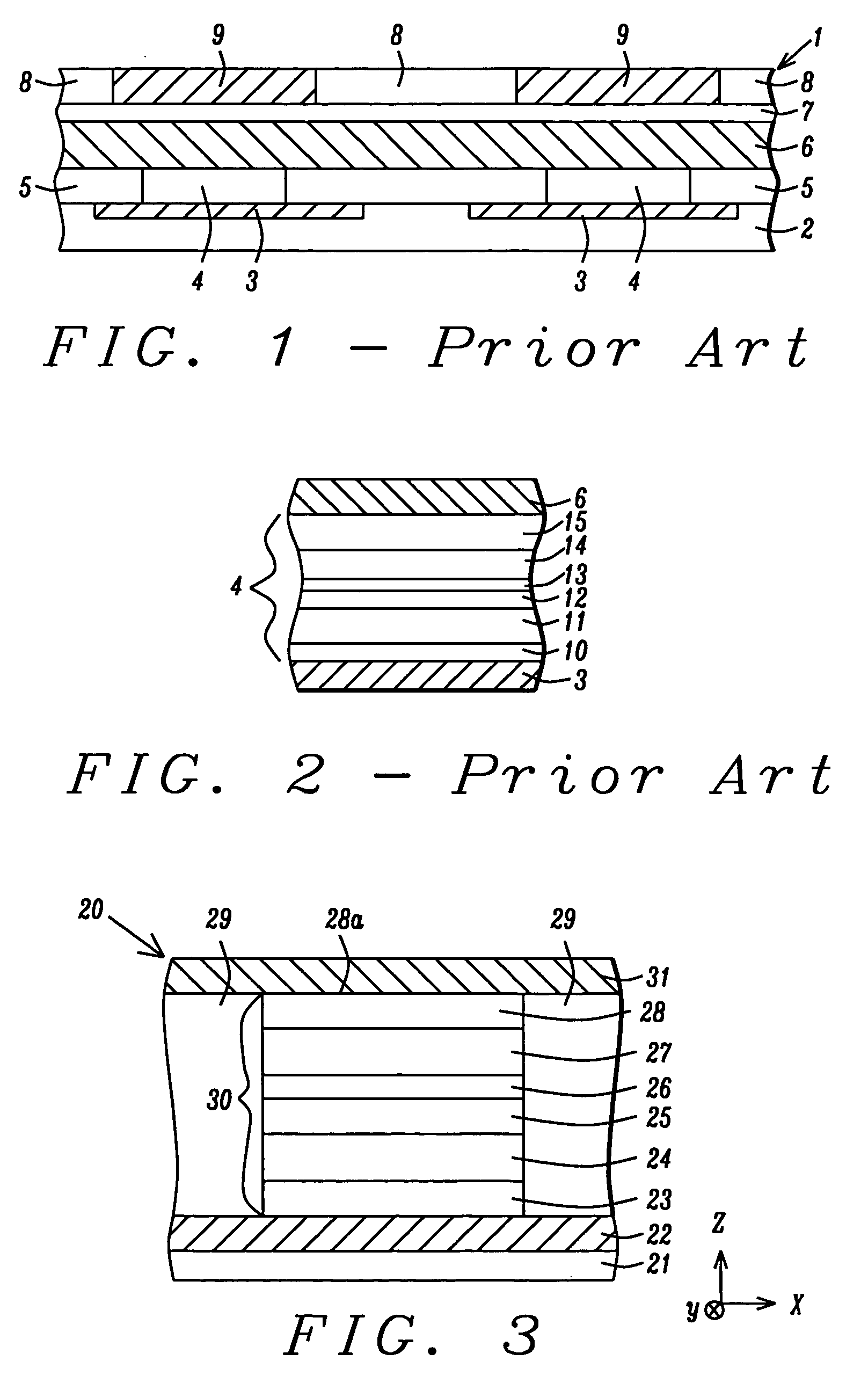
[0032] The present invention is an MRAM structure based on an MTJ in which a free layer and a reference layer have a vortex magnetization state with a net magnetic moment of about zero that is induced and switched by applying a first magnetic field in a first direction and then a smaller magnetic field in an opposite direction. The drawings are provided by way of example and are not intended to limit the scope of the invention. Although only one MRAM cell is depicted in the drawings, it is understood that there are a plurality of MRAM cells in an array that has multiple rows and columns on an MRAM chip. While the exemplary embodiment relates to an MTJ with a bottom spin valve configuration, those skilled in the art will appreciate that the present invention also applies to a top spin valve configuration.

[0033] Referring to FIG. 3, a portion of an MRAM structure 20 is shown that includes a substrate 21 which may be silicon or another semiconductor substrate used in the art. The subs...


PUM


Abstract

An MTJ is disclosed in which the free layer and reference layer have a vortex magnetization state that is formed with a clockwise or counterclockwise rotation. The MTJ has a low aspect ratio elliptical shape and the magnetic layers have a dopant that is one of C, N, B, Zr, Ta, Pt, Nb, or Hf to facilitate the flux closure configuration. The vortex magnetization is induced by applying a reverse magnetic field in a direction opposite to the remnant magnetization in a magnetic layer. An anti-ferromagnetic layer is set in an AFM phase after the vortex state is induced in the adjacent reference layer. Switching the vortex state in the free layer involves applying a first field in a first direction to break the vortex and then applying a smaller second field in a reverse direction to a critical point where a vortex of opposite spin is induced.

Description

FIELD OF THE INVENTION [0001] The invention relates to an MRAM cell structure, and more particularly, to a magnetic tunnel junction (MTJ) that has a low aspect ratio elliptical shape in which a free layer and reference layer have a vortex state of magnetization. The resulting flux closure configuration allows a smaller MRAM cell for dense arrays. BACKGROUND OF THE INVENTION [0002] Magnetic random access memory (MRAM) that incorporates an MTJ as a memory storage device is a strong candidate to provide a high density, fast (1-30 ns read / write speed), and non-volatile solution for future memory applications. An MRAM array is generally comprised of an array of parallel first conductive lines on a horizontal plane, an array of parallel second conductive lines on a second horizontal plane spaced above and formed in a direction perpendicular to the first conductive lines, and an MTJ interposed between a first conductive line and a second conductive line at each crossover point. A first con...

Claims


Application Information

Patent Timeline
Patent Type & Authority Applications(United States)
IPC IPC(8): G11C11/14
CPCG11C11/16G11C11/161G11C11/1675G11C11/15
Inventor MIN, TAIGUO, YIMINWANG, POKANG
Owner HEADWAY TECH INC
Why Eureka
Try Eureka