Antenna device and communication terminal device

a technology of communication terminal and antenna device, which is applied in the direction of resonant antenna, substantially flat resonant element, instrument, etc., can solve the problems of increased production cost, increased production cost, and inability to consider a decrease in mechanical strength, so as to reduce the electric field shielding effect, reduce the mechanical strength, and eliminate the effect of design restrictions

Active Publication Date: 2014-07-24
MURATA MFG CO LTD
View PDF3 Cites 41 Cited by
  • Summary
  • Abstract
  • Description
  • Claims
  • Application Information

AI Technical Summary

Benefits of technology

[0029]According to various preferred embodiments of the present invention, the problems of decreased mechanical strength, design restrictions, and decreased electric field shielding effect are eliminated or avoided since the conductive members are used as a radiator element without providing a slit or opening in a conductor plane of the conductive member.

Problems solved by technology

This creates a problem such that communication with a counterpart antenna becomes difficult to perform.
However, it is necessary to consider a decrease in mechanical strength due to formation of a slit or opening portion in the metal plate.
This costs more man-hours in production.
Particularly, when a slit or opening is formed in a metal casing, there may be an additional constraint on casing design.
This creates a problem such that an electric field shielding effect by the metal plate may be weakened, or a concern such that a first conductor plane and a second conductor plane may interfere with another high frequency circuit.

Method used


Image

  • Antenna device and communication terminal device
  • Antenna device and communication terminal device
  • Antenna device and communication terminal device

Examples


first preferred embodiment

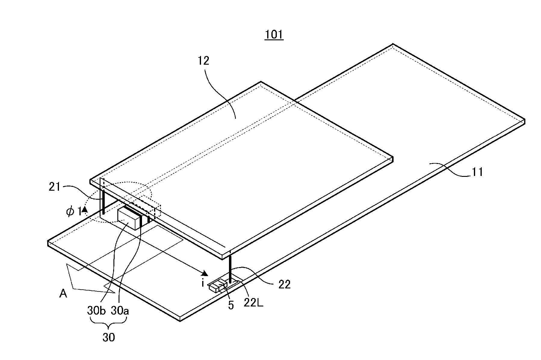
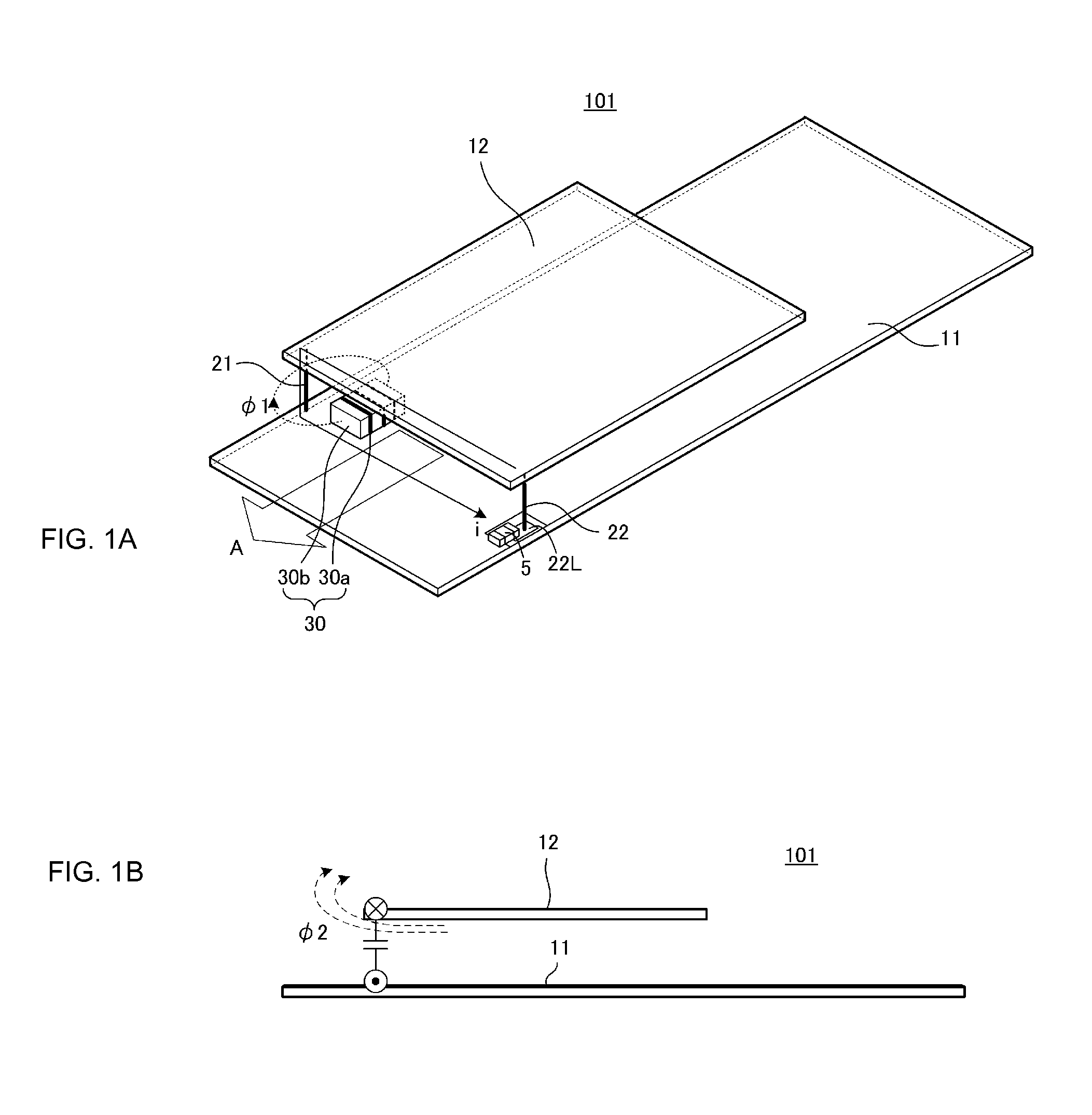
[0067]FIG. 1A is a perspective view of an antenna device 101 according to the first preferred embodiment, and FIG. 1B is a side view of the antenna device 101. The antenna device 101 preferably is an antenna that may be used in HF bands such as, for example, 13.56 MHz and the like, and have proximity type or vicinity type magnetic field coupling with a counterpart antenna.

[0068]The antenna device 101 includes a first conductor plane 11 and a second conductor plane 12 that face each other. The first conductor plane 11 and the second conductor plane 12 that are facing each other are conductive members originally equipped in a communication terminal, and are not prepared for the antenna for use in a HF band communication system. Further, the antenna device 101 includes a first connection conductor 21 and a second connection conductor 22. A power feed coil 30 is disposed between the first conductor plane 11 and the second conductor plane 12. This power feed coil 30 is disposed at a posi...

second preferred embodiment

[0079]FIG. 3 is a perspective view of an antenna device 102 according to the second preferred embodiment of the present invention. A difference from the antenna device 101 illustrated in FIG. 1 in the first preferred embodiment is in the spatial relationship of a power feed coil 30 relative to a first connection conductor 21. In the example illustrated in FIG. 1, the power feed coil 30 is arranged so that a coil winding axis is perpendicular or substantially perpendicular to an opening plane located between the first conductor plane 11 and one side of the second conductor plane 12. On the other hand, in the antenna device 102 of FIG. 3, the power feed coil 30 is arranged so that the coil winding axis is parallel or substantially parallel to the opening plane located between the first conductor plane 11 and one side of the second conductor plane 12. However, the feature that the power feed coil 30 is magnetically coupled with the first connection conductor 21 is preferably the same a...

third preferred embodiment

[0081]FIG. 4A is a perspective view of an antenna device 103 according to the third preferred embodiment of the present invention, and FIG. 4B is an A-A cross-section view of FIG. 4A. The antenna device 103 includes a first conductor plane 11 and a second conductor plane 12 that face each other. A first connection conductor 21 connects the first conductor plane 11 and the second conductor plane 12. A power feed coil 30 is disposed between the first conductor plane 11 and the second conductor plane 12. The first conductor plane 11 may be, for example, a ground conductor pattern of a circuit board. The second conductor plane 12 may be, for example, a metal portion of a casing. The second conductor plane 12 may be, for example, a metal portion configured so as to extend across the range from a flat surface to both side surfaces of the casing. In this example, the first connection conductor 21 is located at a position little behind an opening plane located between an edge side of the se...


PUM


Abstract

An antenna device includes a first conductor plane and a second conductor plane that face each other. The first conductor plane and the second conductor plane are electrically continuous through a first connection conductor, a second connection conductor, and a chip capacitor. A power feed coil is disposed between the first conductor plane and the second conductor plane. The power feed coil includes a magnetic core and a coil conductor. The coil conductor defines a pattern such that the coil conductor winds around the magnetic core. The power feed coil is disposed at a position closer to the first connection conductor and magnetically couples with the first connection conductor.

Description

BACKGROUND OF THE INVENTION[0001]1. Field of the Invention[0002]The present invention relates to antenna devices and communication terminal devices for use in HF band or UHF band telecommunication systems.[0003]2. Description of the Related Art[0004]Typically, in a 13.56 MHz band RFID system such as near field communication (NFC) and the like implemented in cellular phone terminals, a RFID IC chip and matching elements are mostly mounted on a printed wiring board, an antenna is pasted on an inner side surface of a terminal casing, and the IC chip is electrically (galvanically) connected to the antenna with a spring pin or the like.[0005]On the other hand, recent radio communication terminals such as cellular phone terminals are made thinner, and in more cases, the terminal casing is “metalized” by performing, for example, magnesium plating processing on the terminal casing to compensate insufficient strength due to the thinner structure.[0006]However, when the terminal casing is “me...

Claims


Application Information

Patent Timeline
Patent Type & Authority Applications(United States)
IPC IPC(8): H01Q1/52H01Q7/00
CPCH01Q7/00H01Q1/521H01Q1/243G06K19/07794H01Q1/48H01Q9/0407H01Q9/045
Inventor NAKANO, SHINICHIYOSUI, KUNIAKIKATO, NOBORU
Owner MURATA MFG CO LTD
Why Eureka
Try Eureka