Parallel concurrent test system and method

a parallel, test system technology, applied in the direction of electronic circuit testing, measurement devices, instruments, etc., can solve the problems of limiting the return on investment of such equipment, reducing the reliability of automation, and reducing the efficiency of automation, so as to achieve long test time, short test time, and high pin count

Active Publication Date: 2014-08-07
CELERINT
View PDF57 Cites 21 Cited by
  • Summary
  • Abstract
  • Description
  • Claims
  • Application Information

AI Technical Summary

Benefits of technology

[0012]A system and method is provided for conducting a Parallel Concurrent Test (PCT) using automated and robotic semiconductor test equipment. As used herein, PCT testing generally refers to a process of re-configuring a typical sequential test flow for complex semiconductor devices, which have a high pin count and a correspondingly long test time, into a more efficient test flow that utilizes parallel concurrent testing resulting in a significantly shorter test time. PCT testing encompasses a two-pass test flow that is efficiently executed by running the testing on a single, integrated handler. The integrated handler can be configured as a Standard Test Data (STD) handler. Even greater operational efficiencies can be attained by configuring the handler as a Dual Manipulator (DM) handler. These configurations permits a PCT test cell to achieve substantial benefits, including reduced testing time, increased testing device utilization, and increased throughput of the test cell.

Problems solved by technology

Moreover, such automation has increased reliability and results.
A downside of automation has been timing delays in equipment operations.
Particularly, where expensive manufacturing equipment is involved, delays in operations of the equipment, such as during mechanical movements in transferring devices under test, limits returns on the costs of such equipment because of idle or non-testing use periods during mechanical manipulations, resets, and the like.
In semiconductor manufacture, semiconductor device test equipment is a costly capital requirement.
These mechanical manipulations are limited in speed of operations by various factors, including, for example, physical and speed constraints to ensure that devices to be tested are not damaged, contaminated, dropped, and the like.
Although speeds of mechanical operations in handling the test devices have increased significantly over time, there nonetheless remains significant mechanical index time required to manipulate test devices between tests, by the robotic handlers.
Moreover, with increased speeds of mechanical manipulation equipment operations, costs increase for the equipment, including calibration, replacement frequency, maintenance, parts, and others.
Given the constraints and precautions that must be addressed in speeding mechanical manipulations of many types of test devices and handlers, further speeding of mechanical operations is subject to economic and physical barriers.
In any event, reducing index time can provide greater returns on investments in test equipment, particularly where the test equipment is costly.
The primary reasons for serialized testing include thermal issues that restrict the number and complexity of tests that can be conducted at one time, and the complexity of implementation for non-serialized testing.
However, the significant drawbacks include requiring a long test time due to the relatively poor utilization of the test cell's Automatic Test Equipment System 101.
As a result, the conventional standard test cell 100 provides a low throughput resulting in high semiconductor test costs.
Such semiconductor devices conventionally require a long test time.
However, this form of concurrent testing cannot be performed on all test systems and creates thermal management issues due to the increased heat caused by the concurrent testing.
Instead, this type of concurrent testing would need a more complex and expensive ATE system and require higher maintenance than the previously described conventional standard flow test cell.
While simultaneous concurrent testing better utilizes the ATE system, it is characterized by many of the same drawbacks as the previously described concurrent testing of semiconductor devices.
Additionally, high pin count semiconductor devices are limited in how many can be tested concurrently.
Thus, this form of testing reduces the overall test time per semiconductor device compared to the previously described forms of concurrent testing.
DFT pins are typically multiplexed with application pins, so frequently DFT tests cannot be executed in parallel with broadside tests.
Additionally, DFT tests typically consume high levels of power.
As a result, DFT testing generates a lot of heat and requires thermal management to prevent thermal runaway and overheating during the DFT testing.
An operational disadvantage of parallel concurrent testing utilizing an STD handler is that the test time for each test equals the longest test time for each test of the semiconductors being concurrently tested.
The ATE test system is generally characterized by operating at high speed, utilizing a high pin count, and having a high cost.
The integrated PCT test system is generally characterized by operating at a high speed, utilizing a high pin count, and having a relatively high cost.
Additionally, the illustrations are merely representational and may not be drawn to scale.

Method used


Image

  • Parallel concurrent test system and method
  • Parallel concurrent test system and method
  • Parallel concurrent test system and method

Examples


Embodiment Construction

[0054]In view of the foregoing, the present disclosure, through one or more of its various aspects, embodiments and / or specific features or sub-components, is thus intended to bring out one or more of the advantages as specifically noted below. The present disclosure provides a description of a control system and related methodology for conducting efficient Parallel Concurrent Test (PCT) semiconductor testing using automated and robotic semiconductor test equipment.

[0055]In general, the exemplary embodiments disclosed herein involve semiconductor devices being tested that are generally characterized as having a high complexity and a high pin count. Such semiconductor devices conventionally require a long test time. Additionally, the handler(s) referred to herein generally refer to Pick-and-Place (PnP) handlers, and not to gravity feed handlers.

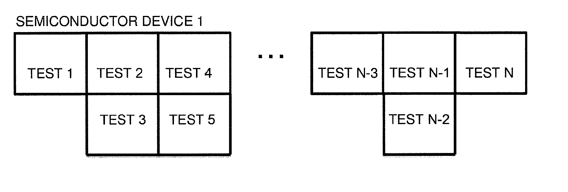
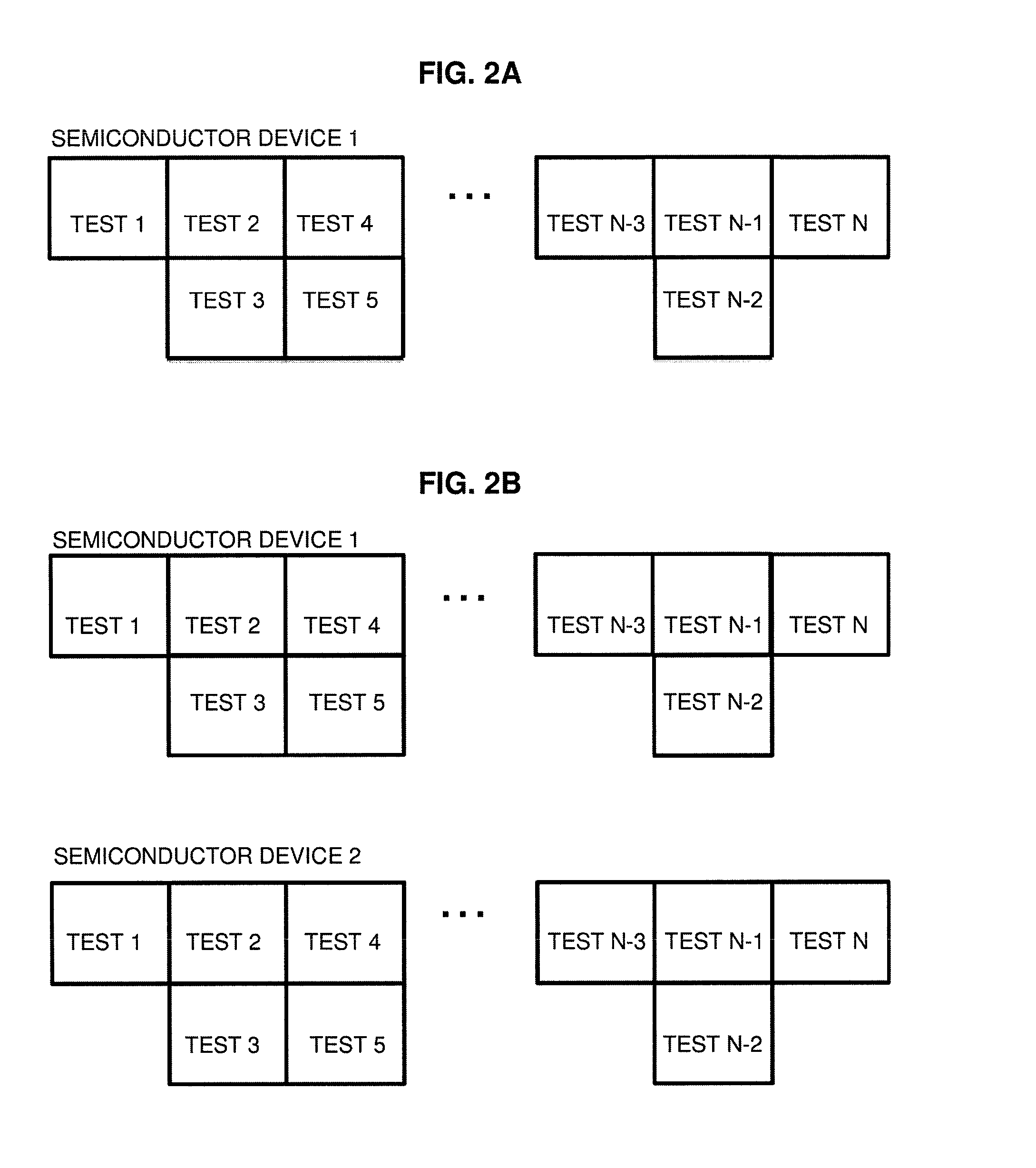
[0056]An exemplary non-limiting illustration of a concurrent testing process is illustrated in FIG. 2A. In this figure, Test 2 and Test 3 are...


PUM


Abstract

A parallel concurrent test (PCT) system is provided for performing the parallel concurrent testing of semiconductor devices. The PCT system includes a pick and place (PnP) handler for engaging and transporting the semiconductor devices along a testing plane, the PnP handler including at least one manipulator. The PCT system also includes a device under test interface board (DIB), the DIB including a broadside test socket for broadside (BS) testing of the semiconductor devices, the broadside testing using at least half of a total number of a semiconductor device pins, and a plurality of design-for-test (DFT) test sockets for DFT testing, the DFT testing using less than half of the total number of the semiconductor device pins, and a tester in electrical contact with the DIB for testing the semiconductor devices in accordance with a stepping pattern test protocol.

Description

CROSS-REFERENCE TO RELATED APPLICATION[0001]This application claims priority for U.S. Provisional Patent Application No. 61 / 487,993, entitled Parallel Concurrent Test System and Method, filed on May 19, 2011, which is incorporated herein in its entirety.TECHNICAL FIELD[0002]The present disclosure relates to automated manufacture systems and methods, particularly automated and robotic semiconductor equipment systems and methods, for testing and manufacture quality control of semiconductors, wherein index timing delays and the overall testing time are reduced.BACKGROUND[0003]Automated manufacturing equipment has streamlined the manufacturing process in many industries. Moreover, such automation has increased reliability and results. A downside of automation has been timing delays in equipment operations. Particularly, where expensive manufacturing equipment is involved, delays in operations of the equipment, such as during mechanical movements in transferring devices under test, limit...

Claims


Application Information

Patent Timeline
Patent Type & Authority Applications(United States)
IPC IPC(8): G01R31/26
CPCG01R31/2601G01R31/2834G01R31/2893G01R31/2865
Inventor ROBERTS, JR., HOWARD H.
Owner CELERINT
Why Eureka
Try Eureka