Touch panel
a technology of touch panel and electrode layer, applied in the field of touch panel, can solve problems such as circuit breakage in the electrode layer, and achieve the effect of reducing the height difference between the visual masking layer and the display area covered by the electrode layer and improving the yield rate of the touch panel
- Summary
- Abstract
- Description
- Claims
- Application Information
AI Technical Summary
Benefits of technology
Problems solved by technology
Method used
Image
Examples
Embodiment Construction
[0027]Reference will now be made in detail to the present preferred embodiments of the invention, examples of which are illustrated in the accompanying drawings. Wherever possible, the same reference numbers are used in the drawings and the description to refer to the same or like parts.
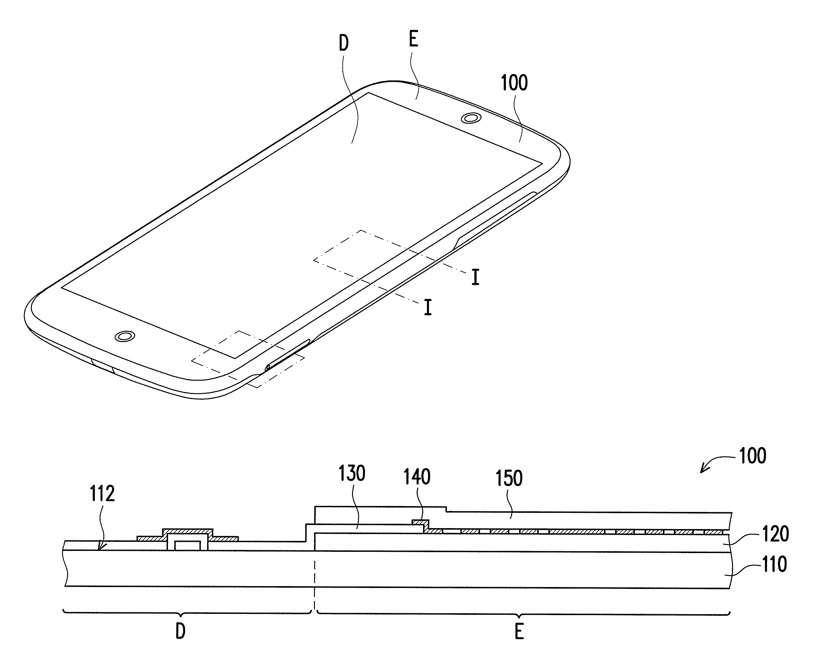
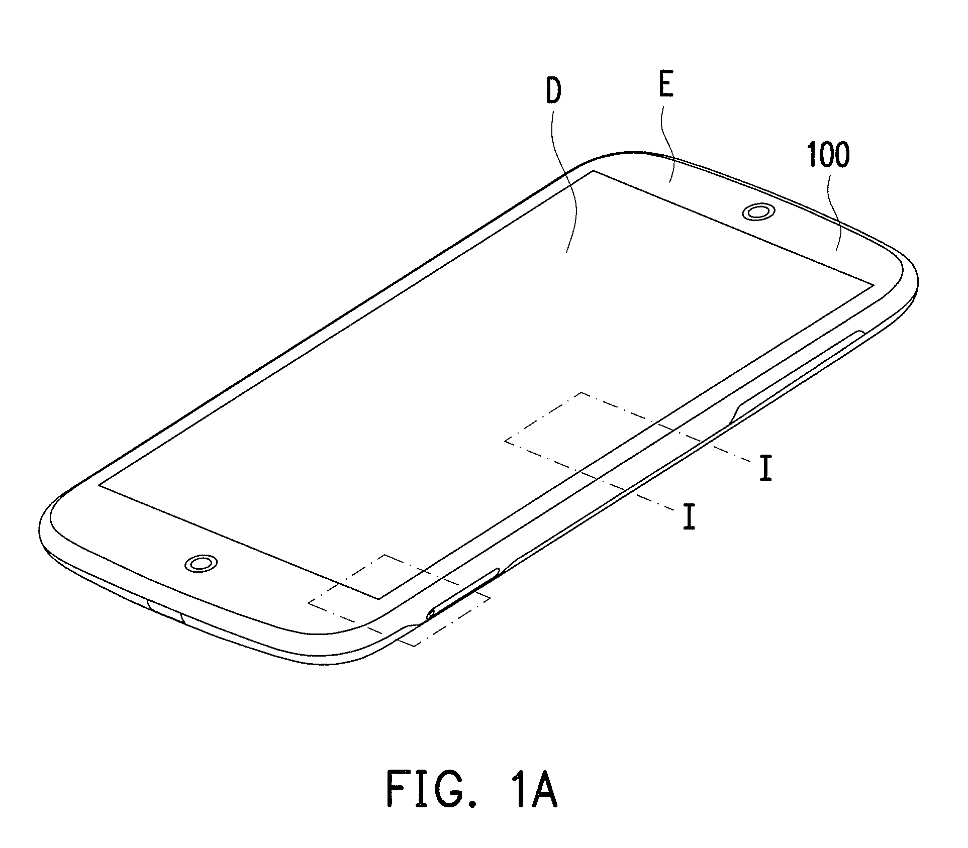
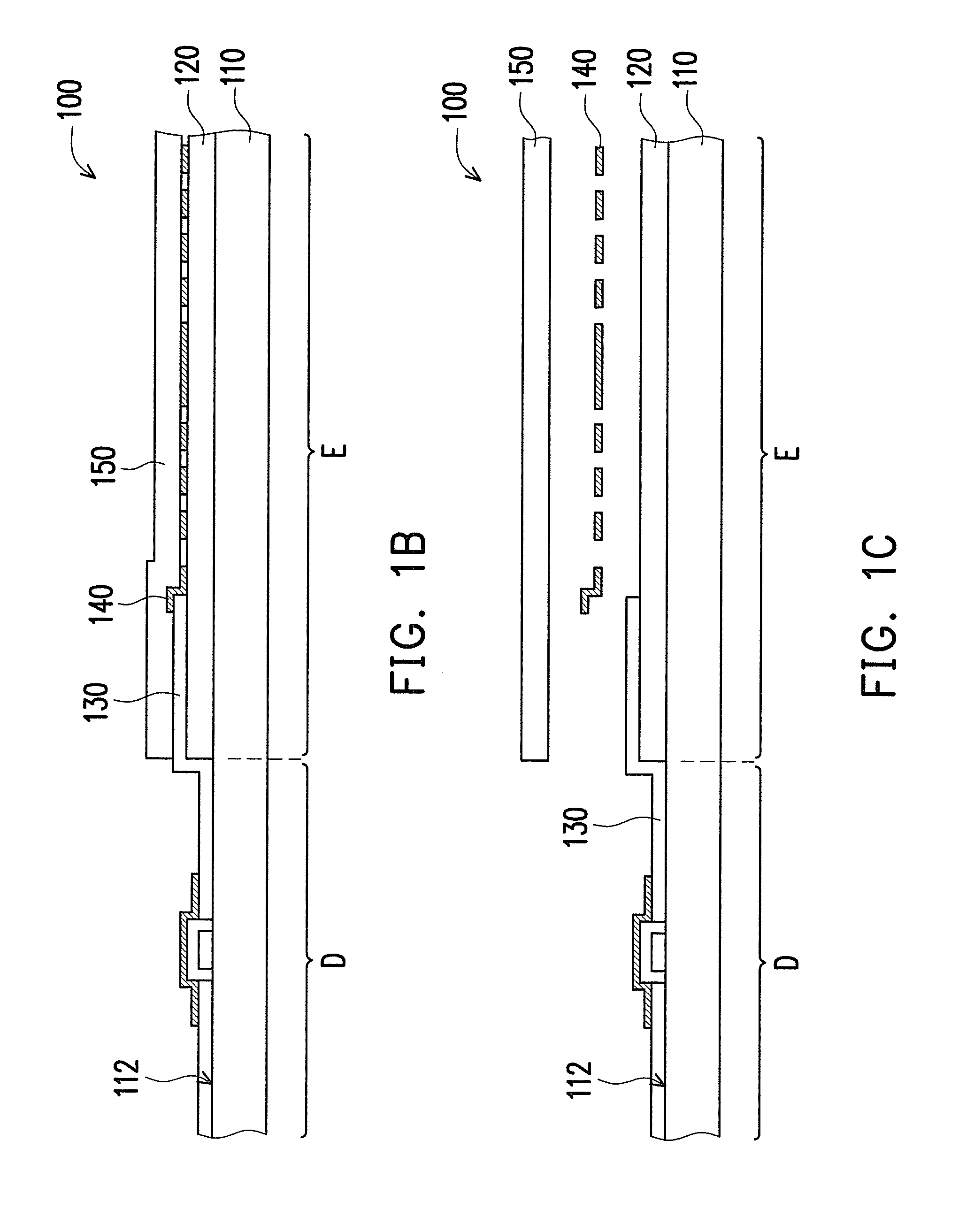
[0028]FIG. 1A is a diagram of a touch panel according to an embodiment of the present invention. FIG. 1B is a cross-sectional view of the touch panel in FIG. 1A along line I-I. FIG. 1C is an exploded view of the touch panel in FIG. 1B. Referring to FIGS. 1A-1C, the touch panel 100 in the present embodiment provides a touch signal. The touch panel 100 includes a substrate 110, a first visual masking layer 120, an electrode layer 130, a metal material layer 140, and a second visual masking layer 150. The substrate 110 has a surface 112. The first visual masking layer 120 is disposed on at least one edge area E of the surface 112.
[0029]After the first visual masking layer 120 is disposed, the electrode ...
PUM
 Abstract
Description
Claims
Application Information


