Touching display panel and display device using the same
a display panel and display device technology, applied in the field of display panel and display device using the same, can solve the problems of difficult to arrange the control circuit board, the total thickness accumulated by all the glass substrates is quite formidable, etc., to achieve optimal circuit planning and design, reduce the number of substrates, and reduce the thickness of the touching display panel
- Summary
- Abstract
- Description
- Claims
- Application Information
AI Technical Summary
Benefits of technology
Problems solved by technology
Method used
Image

Examples
first embodiment
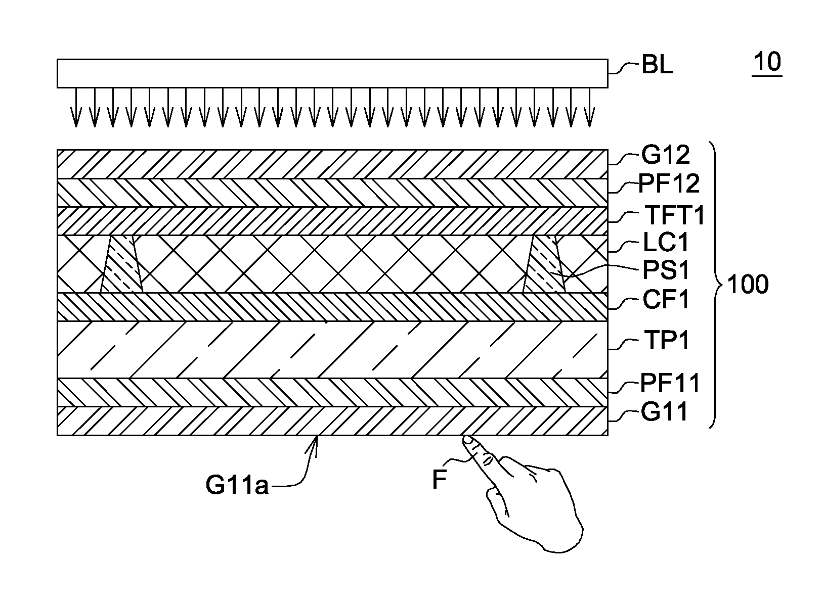
[0018]Referring to FIG. 1 showing a schematic diagram of a display device 10 according to a first embodiment, the display device 10 comprises a touching display panel 100 and a backlight module BL providing a light source to the touching display panel 100. The touching display panel 100 comprises a liquid crystal layer LC1, a first glass substrate G11, a second glass substrate G12, a touch sensor layer TP1, a thin-film transistor layer TFT1 and a color filter layer CF1. In this embodiment, the first glass substrate G11 serves as an outmost-layer cover glass, which comes into contact with a user finger F and protects internal components of the display panel 100 from moisture, abrasions and impacts. The second glass substrate G12 is a glass substrate disposed at a front side of the backlight module BL. The first glass G11 comprises a hard surface structure G11a processed by chemically enhanced treatments or physically enhanced treatments. In the chemically enhanced treatments, the fir...
second embodiment
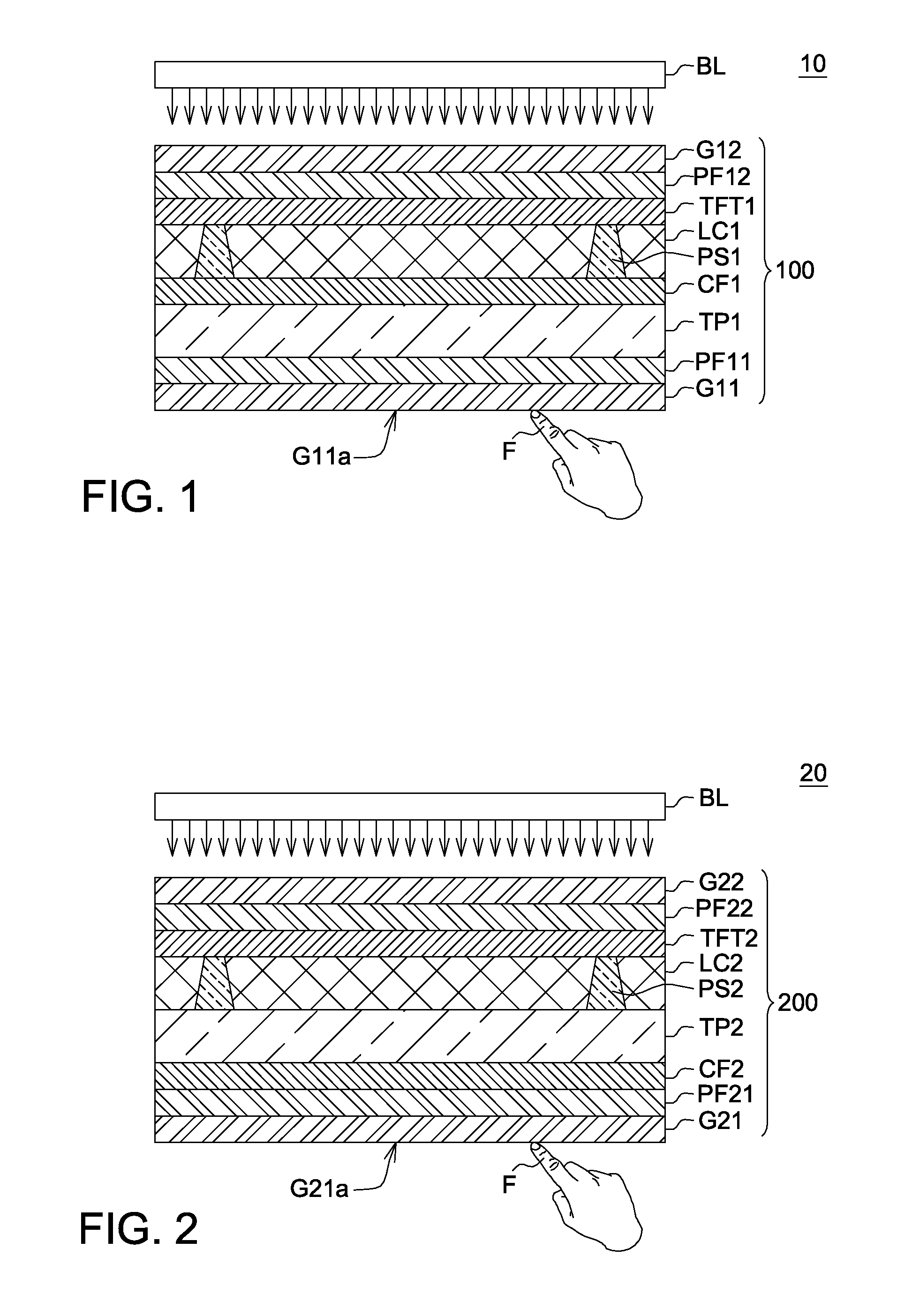
[0024]FIG. 2 shows a schematic diagram of a display device 20 according to a second embodiment. A difference between a touching display panel 200 of the display device 20 in the second embodiment and the touching display panel 100 in the first embodiment is positions of a touch sensor layer TP2 and a color filter layer CF2. More specifically, the color filter layer CF2 of the touching display panel 200 is disposed between a first glass substrate G21 and the touch sensor layer TP2. Details of other correspondingly components are as those previously described and shall not be further given.
[0025]In this embodiment, the thin-film transistor layer TFT2 and the color filter layer CF2 are respectively disposed at two sides of a liquid crystal layer LC2. The touch sensor layer TP2 and the glass filter layer CF2 are joined with a first glass substrate G21 having a hard surface structure G21a through integration, such that a conventional glass substrate used for manufacturing a touch sensor ...
third embodiment
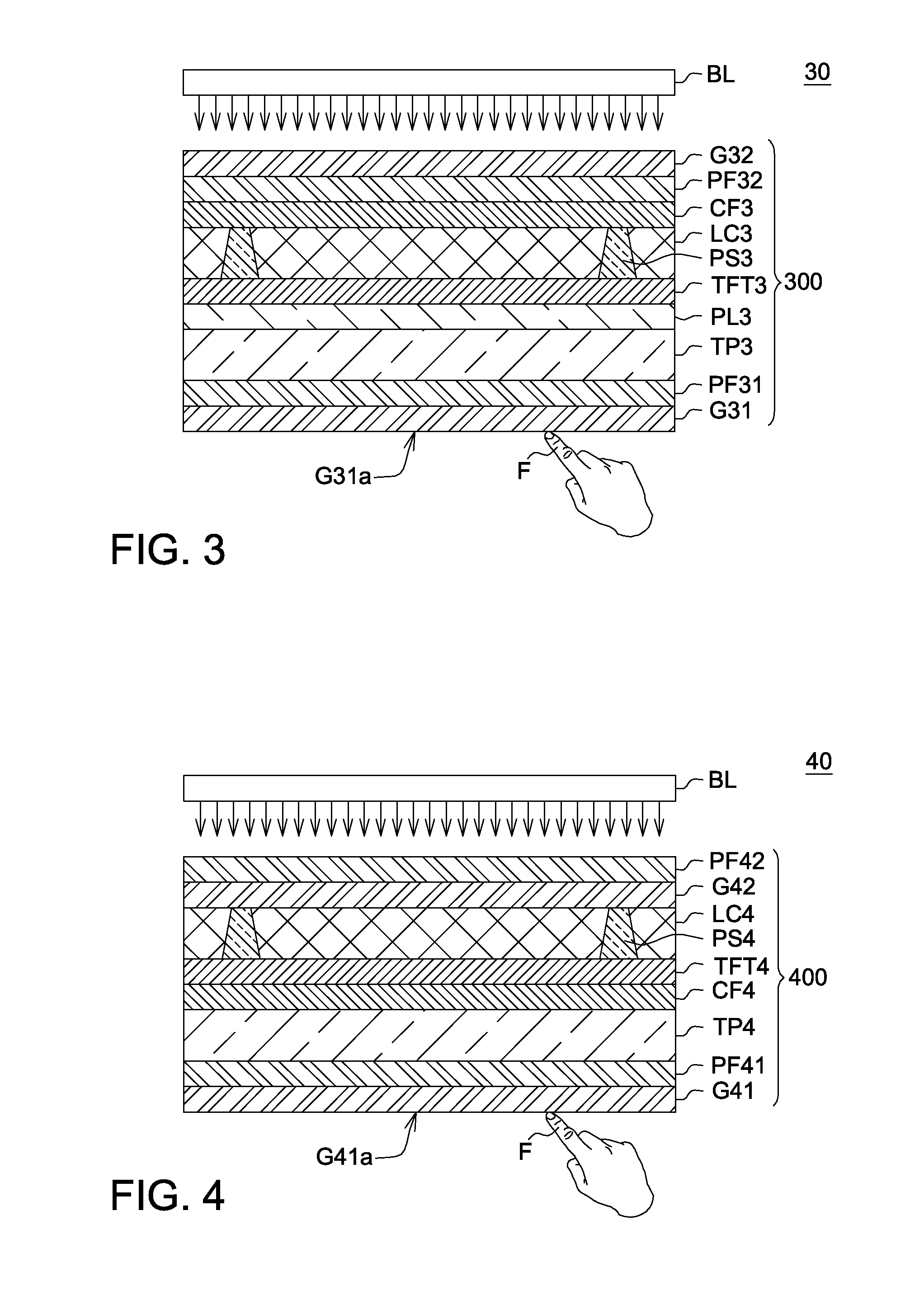
[0029]FIG. 3 shows a schematic diagram of a display device 30 according to a third embodiment of the present disclosure. A difference between a touching display panel 300 of the display device 30 in the third embodiment and the touching display panel 100 in the first embodiment is positions of a thin-film transistor layer TFT3 and a color filter layer CF3. More specifically, the thin-film transistor layer TFT3 is formed on a first glass substrate G31, the color filter layer CF3 is formed on a second glass substrate G32, and a touch sensor layer TP3 is disposed between the first glass substrate G31 and the thin-film transistor layer TFT3. Details of other correspondingly components are as those previously described and shall not be further given.
[0030]Referring to FIG. 3, in the display panel 300 according to this embodiment of the present disclosure, through integration, the thin-film transistor layer TFT3 and the color filter layer CF3 are respectively disposed at two sides of a li...
PUM
| Property | Measurement | Unit |
|---|---|---|
| current | aaaaa | aaaaa |
| hard surface structure | aaaaa | aaaaa |
| volume | aaaaa | aaaaa |
Abstract
Description
Claims
Application Information
 - Generate Ideas
- Intellectual Property
- Life Sciences
- Materials
- Tech Scout
- Unparalleled Data Quality
- Higher Quality Content
- 60% Fewer Hallucinations
Browse by: Latest US Patents, China's latest patents, Technical Efficacy Thesaurus, Application Domain, Technology Topic, Popular Technical Reports.
© 2025 PatSnap. All rights reserved.Legal|Privacy policy|Modern Slavery Act Transparency Statement|Sitemap|About US| Contact US: help@patsnap.com