Current sensing resistor
a resistor and current sensing technology, applied in resistor details, thick film resistors, instruments, etc., can solve the problems of adverse effects on product stability and yield, value and uniformity of resistance, and adverse effects on product yield and stability
- Summary
- Abstract
- Description
- Claims
- Application Information
AI Technical Summary
Benefits of technology
Problems solved by technology
Method used
Image
Examples
first embodiment
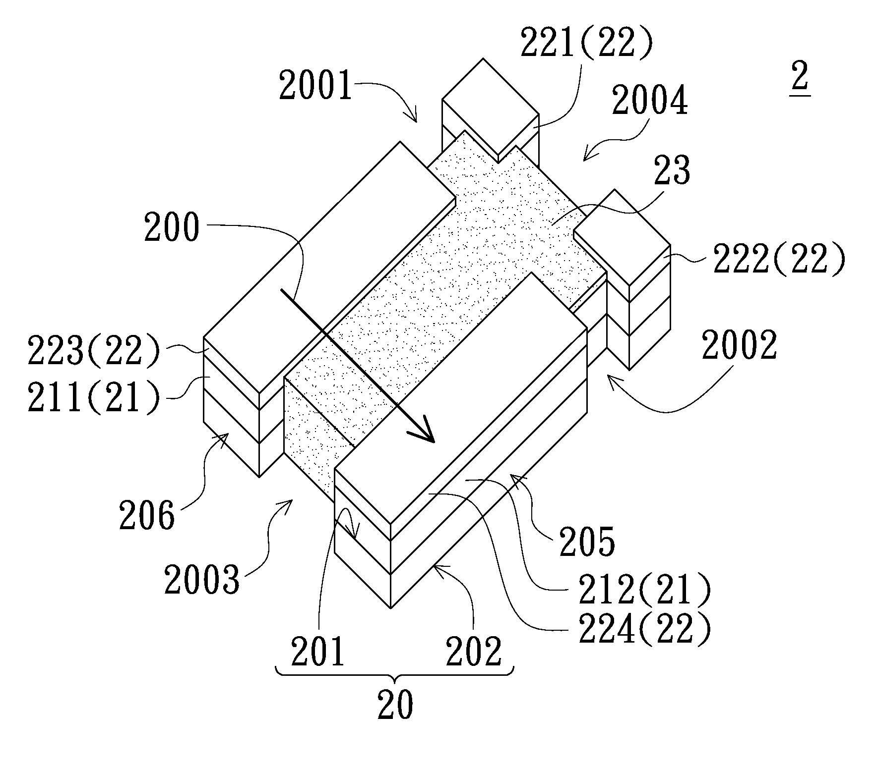
[0040]Please refer to FIG. 3A and FIG. 3B. FIG. 3A is a prospective view schematically illustrating a current sensing resistor device according to the present invention. FIG. 3B is a perspective view schematically illustrating the resistor device of FIG. 3A, in which the protective layer is not shown. In this embodiment, the current sensing resistor device 2 includes a resistor plate 20, a first metal layer 21, a second metal layer 22 and a protective layer 23. The resistor plate 20 has a first face 201 and a second face 202 opposite to the first face 201. The first metal layer 21 is disposed on the first face 201 of the resistor plate 20. As shown in FIG. 3B, the first metal layer 21 includes a first portion 211 and a second portion 212. In practice, the first portion 211 and the second portion 212 are disposed at opposite sides of the first face 201, and current may flow through a current path 200 between the first portion 211 of the first metal layer 21 and the second portion 212...
third embodiment
[0046]Please refer to FIGS. 6A, 6B and 6C, in which a resistor device according to the present invention is shown. The configuration of the resistor device 2b is similar to that of the resistor device 2a shown in FIGS. 4A, 4B and 5 with some modifications. FIG. 6B, in which the protective layer 23 is not shown, is further referred to clearly understand the structure of the resistor device 2b. As shown in FIG. 6C, the first portion 211 and the second portion 212 of the first metal layer 21 of the resistor device 2b have outward opposite sides 213 and inward opposite sides 214, respectively. The distance between each pair of the outward and inward opposite sides 213 and 214 is, for example, W1. On the other hand, portions of the second metal layer 22a of the resistor device 2b separately formed on the first portion 211 and the second portion 212 of the first metal layer 21 have outward opposite sides 215 and inward opposite sides 208 and 209, respectively. The distance between each pa...
fourth embodiment
[0049]Please refer to FIGS. 7, 8 and 9, in which a resistor device according to the present invention is shown. FIG. 8 is a schematic cross-sectional view of the resistor device taken along B-B line of FIG. 7. The configuration of the resistor device 2c is similar to that of the resistor device 2a shown in FIGS. 4A, 4B and 5 with some modifications. The resistor device 2c in this embodiment further includes an auxiliary layer 25 disposed on the resistor plate 20 and defined with four separate blocks 251, 252, 253 and 254, which function for strengthening the entire resistor device and preventing from heat warp. In this embodiment, the blocks 251, 252, 253 and 254 correspond to the first sensing pad 221, the second sensing pad 222, the first current pad 223 and the second sensing pad 224, respectively, and are kept insulated from the pads. Concretely, the blocks 251, 252, 253 and 254 are disposed on the second surface 202 at four corners of the resistor plate 20. In this embodiment, ...
PUM
 Abstract
Description
Claims
Application Information


