

Display device, manufacturing method thereof, and electronic device
a technology of display device and manufacturing method, applied in the direction of thermoelectric device junction materials, semiconductor devices, electrical apparatus, etc., can solve the problem of affecting the display quality of the panel, and achieve the effect of reducing the reflection of external light and high display quality
- Summary
- Abstract
- Description
- Claims
- Application Information
AI Technical Summary
Benefits of technology
Problems solved by technology
Method used
Image

Examples
embodiment 1
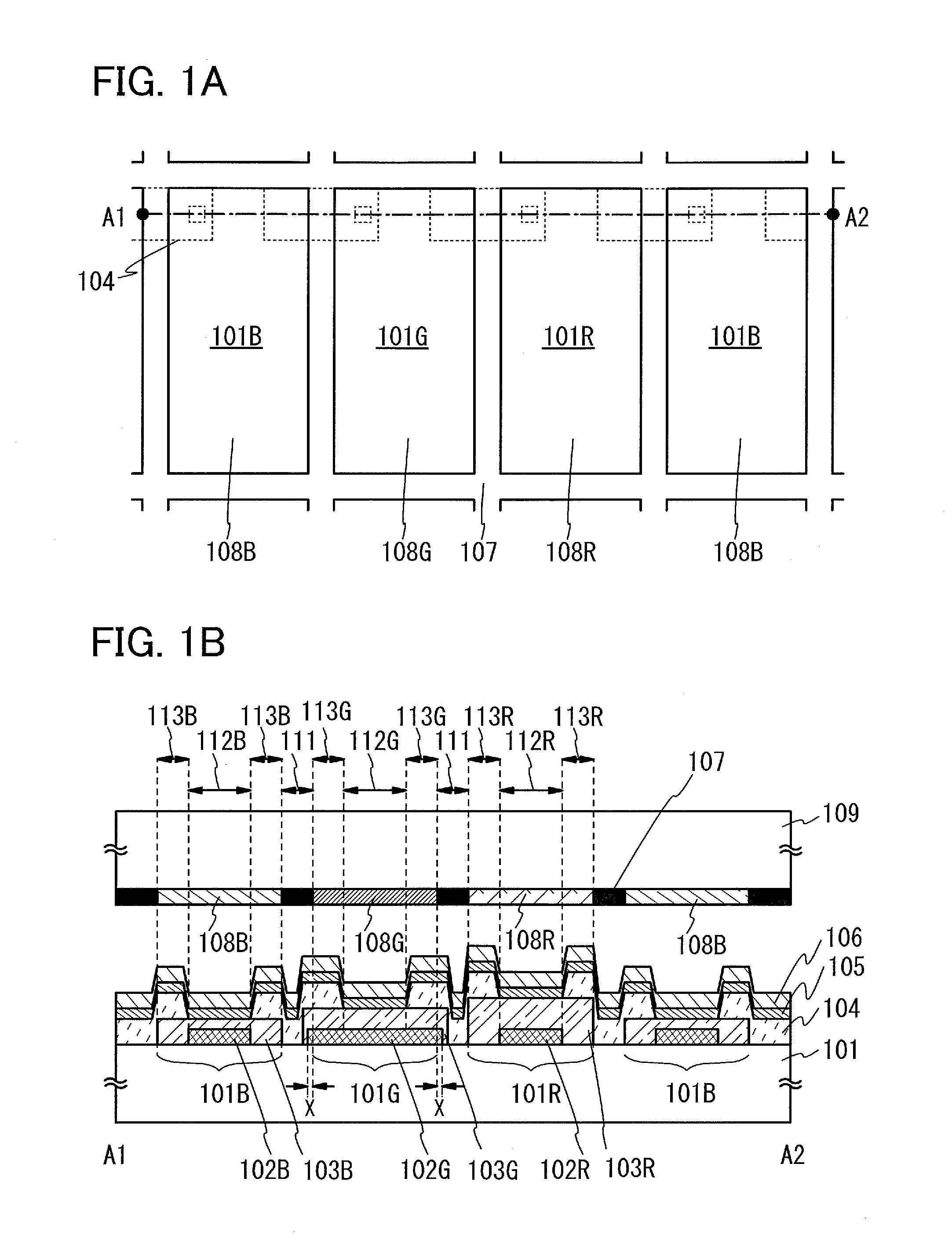
[0047]In this embodiment, a display device of one embodiment of the present invention will be described with reference to FIGS. 1A and 1B.
[0048]A structure example of a display device in this embodiment is illustrated in FIGS. 1A and 1B. FIG. 1A is a top view illustrating part of a pixel region of the display device, and FIG. 1B is a cross-sectional view taken along dashed-dotted line A1-A2 in FIG. 1A. Note that for simplification of the drawing, some components are illustrated in a see-through manner or not illustrated in the top view in FIG. 1A.
[0049]FIG. 1A illustrates part of the pixel region of the display device, in which pixel patterns of a pixel portion (blue), a pixel portion (green), and a pixel portion (red) are arranged in matrix, for example, and each pixel pattern includes an unshown thin film transistor (TFT) which serves as a switching element for switching an on state and an off state of a pixel portion. Note that although the pixel patterns of three colors, i.e., t...
embodiment 2
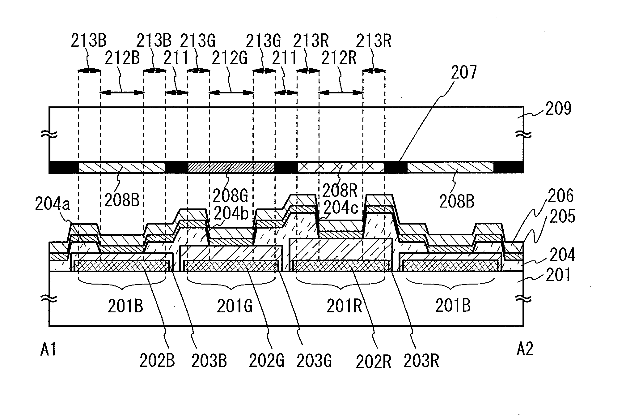
[0070]In this embodiment, for example, a structure illustrated in FIG. 2 can be employed to reduce reflection of external light. FIG. 2 corresponds to a cross section taken along a dashed-dotted line A1-A2 in FIG. 1A.
[0071]With reference to FIG. 2, description is given of a display device which has a structure for reducing the surface reflectance of external light in a non-light-emitting region 213B of a pixel portion (blue) 201B, a non-light-emitting region 213G of a pixel portion (green) 201G, and a non-light-emitting region 213R of a pixel portion (red) 201R.
[0072]Note that in the description below, a BM region 211 in which a black matrix (BM) 207 blocks light, light-emitting regions 212B, 212G, and 212R and the non-light-emitting regions 213B, 213G, and 213R of the pixel portion (blue) 201B, the pixel portion (green) 201G, and the pixel portion (red) 201R are provided over a panel of the display device.
[0073]The display device illustrated in FIG. 2 includes a first substrate 201...
embodiment 3
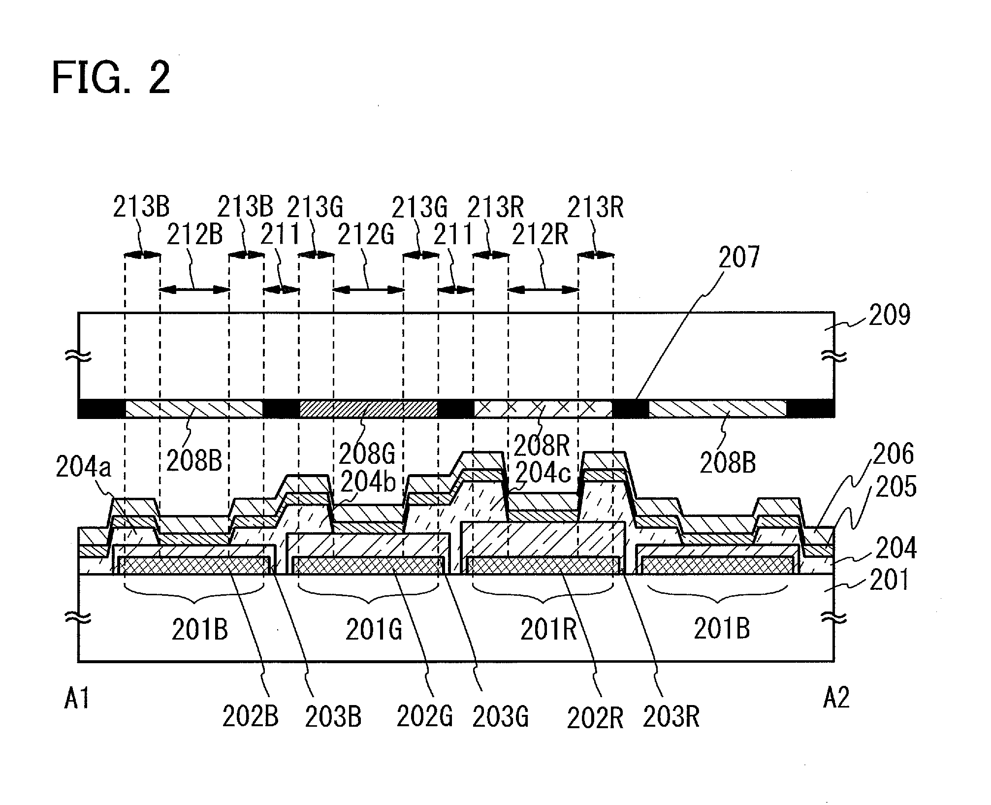
[0089]In this embodiment, thicknesses of the first partition 204a, the second partition 204b, and the third partition 204c in the pixel portions 201B, 201G, and 201R which are described in Embodiment 2 are adjusted by mask vapor deposition. The description will be made with reference to FIG. 3. FIG. 3 corresponds to a cross section taken along a dashed-dotted line A1-A2 in FIG. 1A.
[0090]Note that in the description below, a color filter (blue) 308B, a color filter (green) 308G, a color filter (red) 308R, a BM region 311 in which a black matrix (BM) 307 blocks light, light-emitting regions 312B, 312G, and 312R and non-light-emitting regions 313B, 313G, and 313R of a pixel portion (blue) 301B, a pixel portion (green) 301G, and a pixel portion (red) 301R are provided over a panel of a display device.
[0091]The display device illustrated in FIG. 3 includes a first substrate 301 and a second substrate 309 which are similar to the first substrate 101 and the second substrate 109 illustrate...
PUM
 Abstract
Description
Claims
Application Information