

Optical deflector
a technology of optical deflectors and deflectors, applied in the field of optical deflectors, can solve the problems of reducing diffraction efficiency and difficult control of diffraction angle, and achieve the effect of reducing the short circuit between the transparent electrodes and reducing unnecessary diffracted light during operation
- Summary
- Abstract
- Description
- Claims
- Application Information
AI Technical Summary
Benefits of technology
Problems solved by technology
Method used
Image

Examples
first embodiment
of the Invention
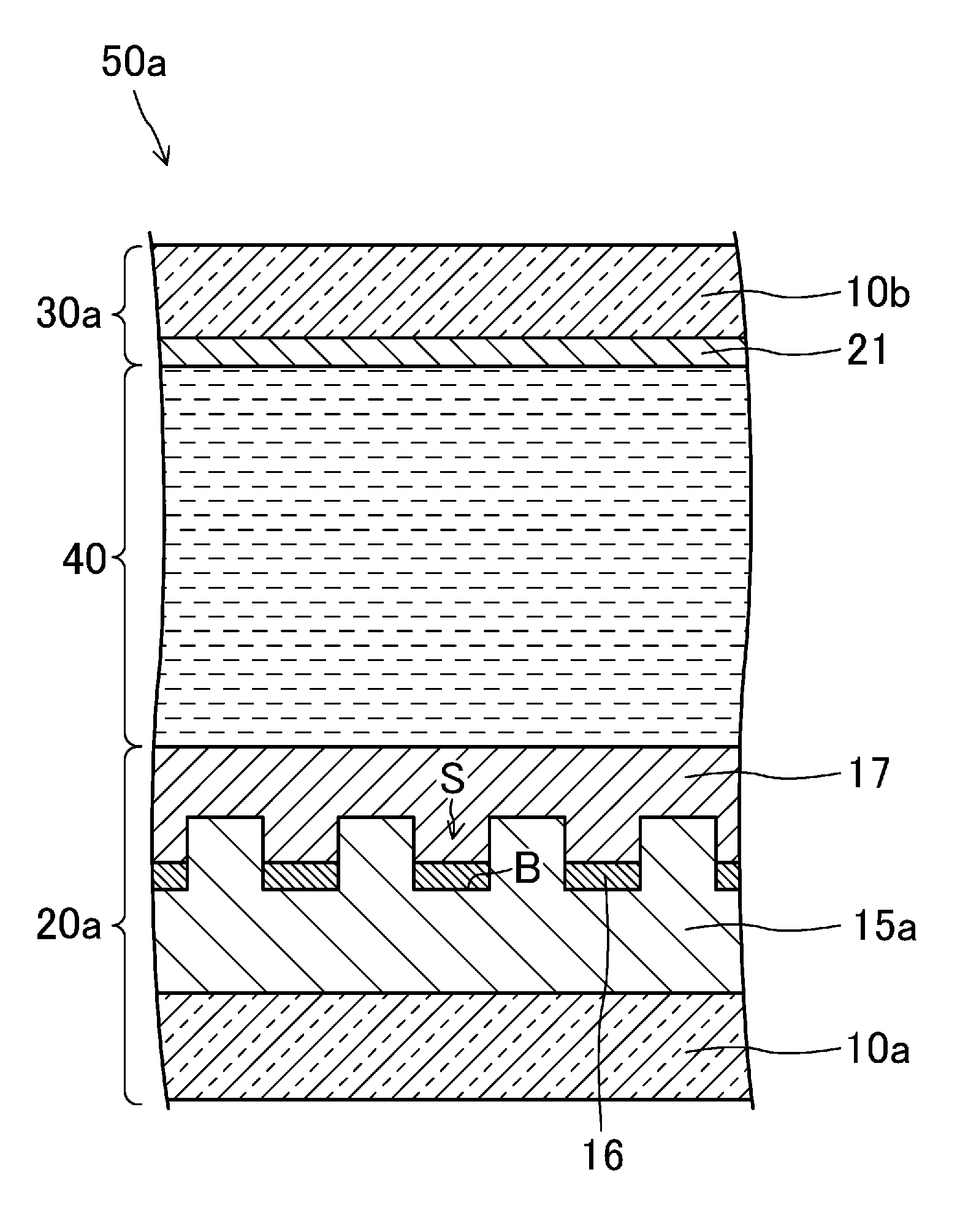
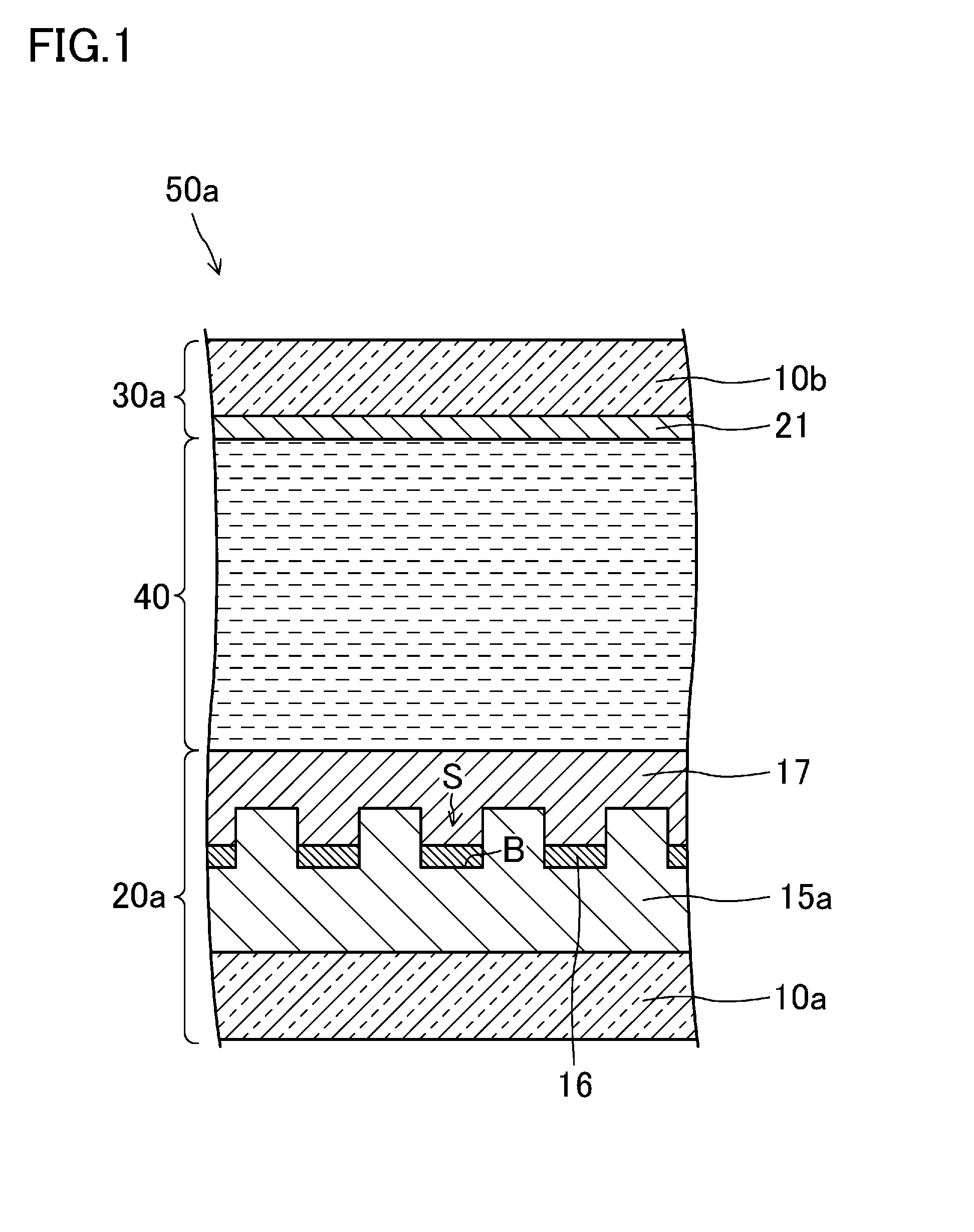
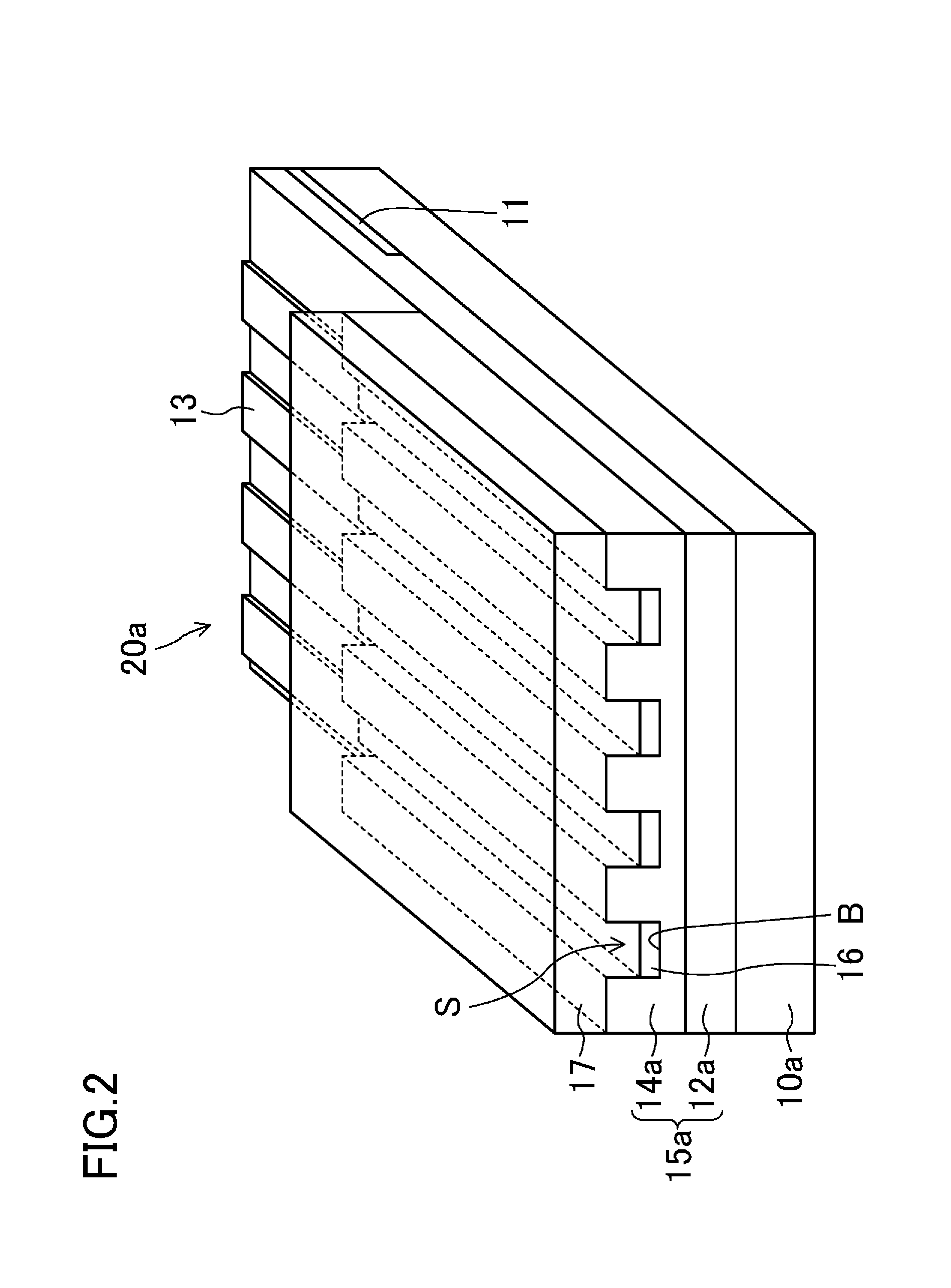
[0065]FIGS. 1-19 illustrate a first embodiment of an optical deflector according to the present invention. Specifically, FIG. 1 is a cross-sectional view illustrating an optical deflector 50a of the present embodiment. FIG. 2 is a perspective view illustrating a first element substrate 20a included in the optical deflector 50a. FIGS. 3-17 which will be described later are views illustrating a method for fabricating the first element substrate 20a, wherein FIG. 8 is a plan view illustrating the first element substrate 20a fabricated by the fabrication method, FIG. 16 is a cross-sectional view illustrating the first element substrate 20a along the line XVI-XVI of FIG. 8, and FIG. 17 is a cross-sectional view illustrating the first element substrate 20a along the line XVII-XVII of FIG. 8.
[0066]As illustrated in FIG. 1, the optical deflector 50a includes the first element substrate 20a and a second element substrate 30a which face each other, a homogeneous alignment type...
second embodiment
of the Invention
[0099]FIGS. 20-27 illustrate a second embodiment of an optical deflector according to the present invention. Specifically, FIG. 20 is a cross-sectional view illustrating an optical deflector 50b of the present embodiment. FIG. 21 is a plan view illustrating a first element substrate 20b included in the optical deflector 50b. FIGS. 22, 23, and 24 are cross-sectional views illustrating the first element substrate 20b respectively along the line XXII-XXII, the line XXIII-XXIII, and the line XXIV-XXIV of FIG. 21. FIG. 25 is a cross-sectional view illustrating a method for fabricating forming a second interlayer insulating layer 14b included in the first element substrate 20b. In the following embodiment, the same reference numerals as those shown in FIGS. 1-19 are used to represent equivalent elements, and the detailed explanation thereof will be omitted.
[0100]The first embodiment has described the optical deflector 50a in which each of the first transparent electrodes 1...
third embodiment
of the Invention
[0114]FIGS. 28-31 illustrate a third embodiment of an optical deflector according to the present invention. Specifically, FIG. 28 is a cross-sectional view illustrating an optical deflector 50c of the present embodiment. FIG. 29 is another cross-sectional view illustrating the optical deflector 50c.
[0115]The first embodiment and the second embodiment have respectively described the optical deflector 50a and the optical deflector 50b including the second element substrate 30a provided with a single second transparent electrode 21. However, the present embodiment will describe the optical deflector 50c including a second element substrate 30c provided with a plurality of second transparent electrodes 27.
[0116]As illustrated in FIG. 28, the optical deflector 50c includes a first element substrate 20a and the second element substrate 30c which face each other, a homogeneous alignment type liquid crystal layer 40 provided between the first element substrate 20a and the s...
PUM
| Property | Measurement | Unit |
|---|---|---|
| thickness | aaaaa | aaaaa |
| thickness | aaaaa | aaaaa |
| depth | aaaaa | aaaaa |
Abstract
Description
Claims
Application Information