Method of manufacturing semiconductor device having plural semiconductor chips stacked one another

a semiconductor chip and semiconductor technology, applied in semiconductor/solid-state device manufacturing, solid-state devices, electric devices, etc., can solve the problems of chip cracks, inability to manage external dimensions, and concern that stress may be applied to thin semiconductor chips, so as to reduce the stress of the underfill material, prevent the variation of the outer shape and improve the resistance of the second chip laminated body

Inactive Publication Date: 2014-10-02
PS4 LUXCO SARL
View PDF4 Cites 10 Cited by
  • Summary
  • Abstract
  • Description
  • Claims
  • Application Information

AI Technical Summary

Benefits of technology

[0013]According to the above aspects of the present invention, it is possible to prevent variation in the outer shape of the second chip laminated body because the fillet portion is trimmed. Therefore, it becomes possible to manage the external dimensions of the second chip laminated body.
[0014]As the external dimensions of the second chip laminated body become stable, the resistance of the second chip laminated body can be improved against the stress resulting from an external force at the time of handling.
[0015]Furthermore, because the fillet portion is trimmed, it is possible to reduce the stress of the underfill material at a time when the second chip laminated body with the underfill material is heated.
[0016]Therefore, it is possible to prevent the breakage or chip cracking of the semiconductor chips that may be made thin (e.g. semiconductor chips with a thickness of 50 μm or less, for example), and the breaking of the connection portions (joint areas) between the semiconductor chips.

Problems solved by technology

Depending on how the fillets have spread, the external dimensions of the chip laminated body (which is, in other words, a structure made up of the underfill material and the chip laminated body), on which the underfill material has been formed, become uneven, making it impossible to manage the external dimensions.
If the above fillets are large, there is concern that stress may be applied to the thin semiconductor chips, which constitute the chip laminated body, as the fillet portions swell and contract each time the chip laminated body is heated in a process of mounting the chip laminated body, on which the underfill material is formed, on the package substrate, and in subsequent processes.
If the stress is applied to the chip laminated body, there is concern that cracks may appear in the chips, or that a bump joint area where the semiconductor chips are connected together may break up.

Method used


Image

  • Method of manufacturing semiconductor device having plural semiconductor chips stacked one another
  • Method of manufacturing semiconductor device having plural semiconductor chips stacked one another
  • Method of manufacturing semiconductor device having plural semiconductor chips stacked one another

Examples


first embodiment

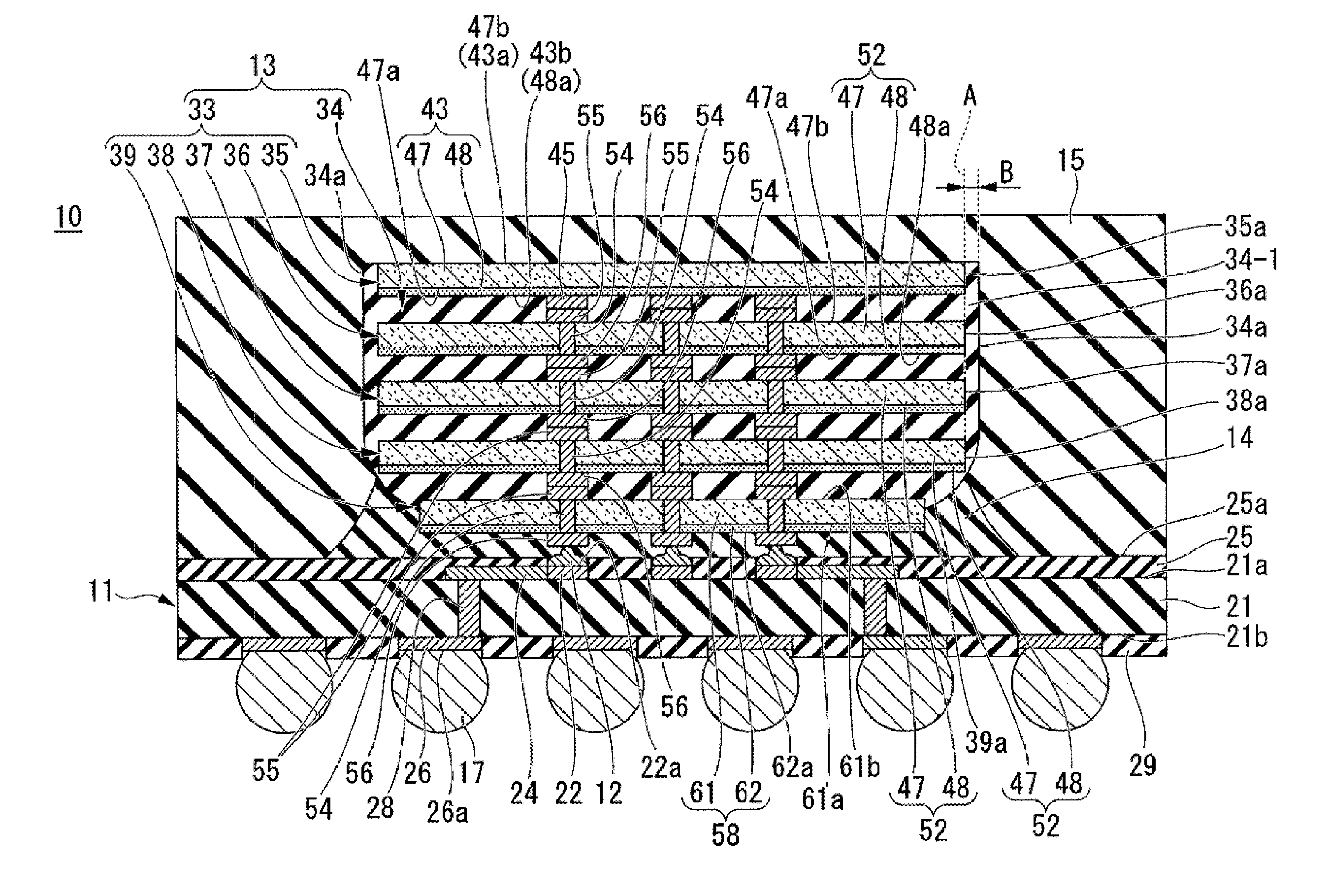
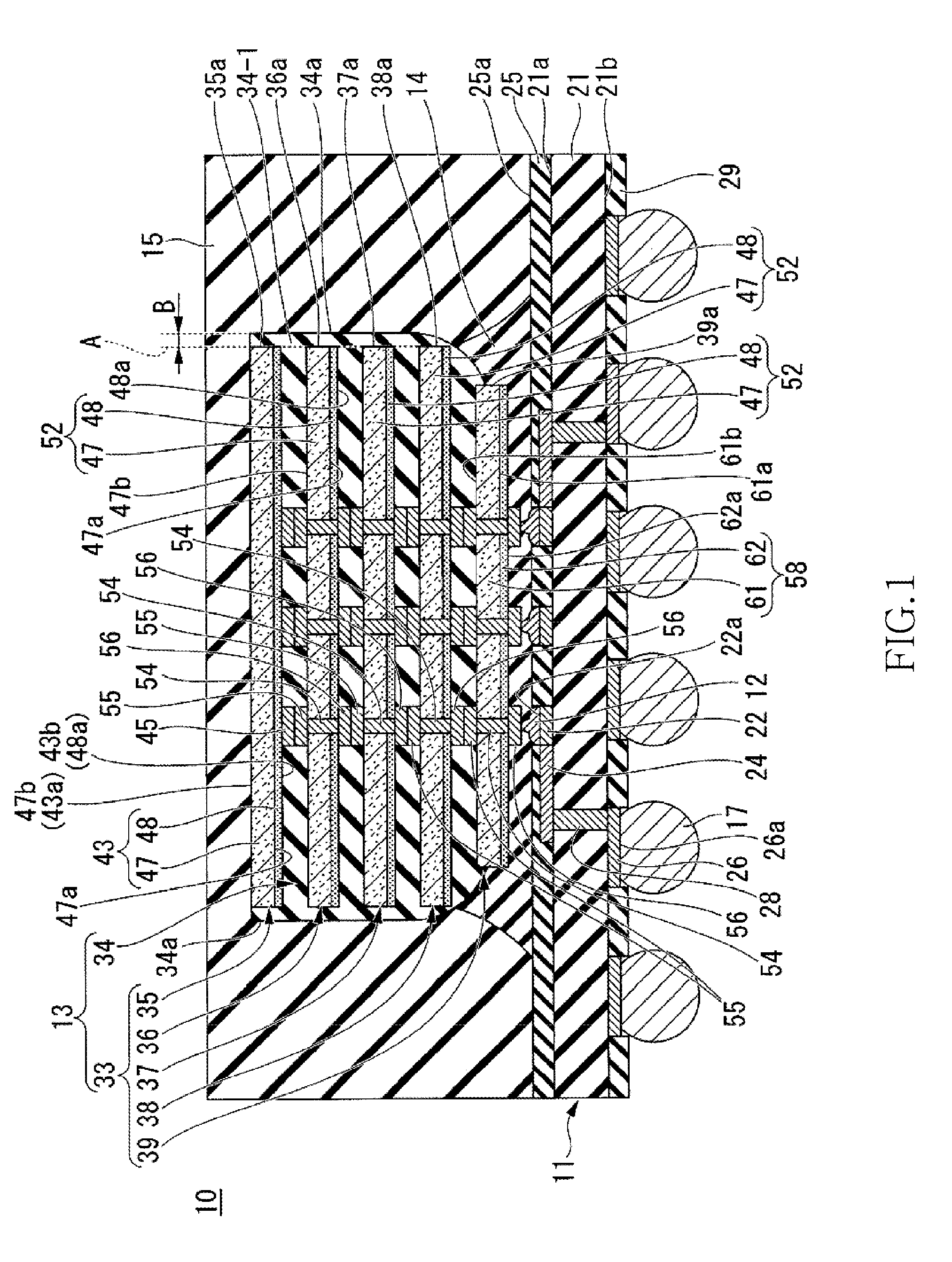
[0025]Referring now to FIG. 1, a semiconductor device 10 of the first embodiment is a semiconductor device of a CoC (Chip on Chip) type. The semiconductor device 10 includes a wiring substrate 11, wire bumps 12, a chip laminated body 13 with an underfill material, a first sealing resin 14, a second sealing resin 15, and external connection terminals 17.

[0026]The wiring substrate 11 includes a wiring substrate body 21, connection pads 22, wirings 24, a first solder resist 25, external connection pads 26, penetration electrodes 28, and a second solder resist 29.

[0027]The wiring substrate body 21 is an insulating substrate that is in the shape of a rectangle, and has a flat surface 21a (principal surface of the wiring substrate 11), and a back surface 21b. For the wiring substrate body 21, for example, a glass epoxy board may be used.

[0028]The connection pads 22 are provided in a central portion of the surface 21a of the wiring substrate body 21. The connection pads 22 are so disposed ...

second embodiment

[0195]A semiconductor device according to a second embodiment of the present invention will be explained with reference to FIG. 17. In FIG. 17, the same components as those of the semiconductor device 10 of the first embodiment are represented by the same reference symbols.

[0196]As shown in FIG. 17, the semiconductor device 110 of the second embodiment has the same configuration as the semiconductor device 10 except that: instead of the wiring substrate 11 that is provided in the semiconductor device 10 of the first embodiment, a wiring substrate 111 is provided; and that a logic semiconductor chip 113, a plurality of metal wires 114, and an adhesive 115 are provided.

[0197]The wiring substrate 111 has the same configuration as the wiring substrate 11 described in the first embodiment except that: the connection pads 22 are disposed at the outer periphery of the surface 21a of the wiring substrate body 21; the wirings 24 are disposed on the back surface 21b of the wiring substrate bo...

third embodiment

[0221]A semiconductor device according to a third embodiment of the present invention will be explained with reference to FIG. 18. In FIG. 18, the same components as those of the semiconductor device 10 of the first embodiment are represented by the same reference symbols.

[0222]As shown in FIG. 18, the semiconductor device 200 of the present embodiment is different from the semiconductor device 100 of the first embodiment shown in FIG. 1 mainly in that: the chip laminated body 13 with the underfill material shown in FIG. 1 is replaced with a chip laminated body 220 with an underfill material; and the second semiconductor chip 39 is replaced with a third semiconductor chip 230.

[0223]The chip laminated body 220 with the underfill material includes a chip laminated body 210 and an underfill material 34.

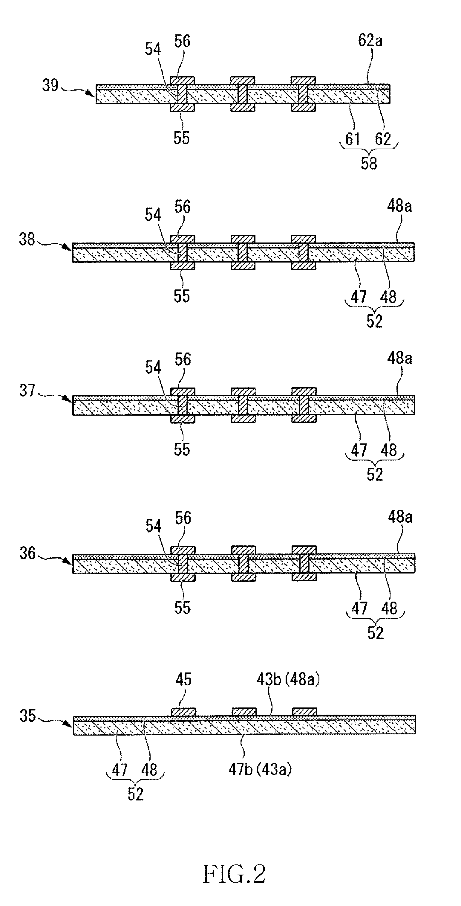
[0224]The chip laminated body 210 is made up of the first semiconductor chip 35 and a plurality of second semiconductor chips 36 to 38. Similarly to the first embodiment, for the semicon...


PUM


Abstract

Disclosed herein is a method of manufacturing a semiconductor device that includes stacking a plurality of semiconductor chips to form a first chip laminated body, providing an underfill material to fill gaps between the semiconductor chips so that a fillet portion is formed around the first chip laminated body, and trimming the fillet portion to form a second chip laminated body.

Description

BACKGROUND OF THE INVENTION[0001]1. Field of the Invention[0002]The present invention relates to a method of manufacturing a semiconductor device, and more particularly to a method of manufacturing a semiconductor device having a plurality of semiconductor chips stacked one another.[0003]2. Description of Related Art[0004]In recent years, the integration density of semiconductor chips has been increasing year after year, leading to an increase in the size of the chips and promoting miniaturization of wiring and multi-layer structures. Meanwhile, in order to realize high-density mounting, the semiconductor devices need to be made smaller in size and thinner.[0005]To meet such a need, a technique called MCP (Multi Chip Package) has been developed of mounting a plurality of semiconductor chips on one package substrate in a high-density manner.[0006]Especially, the semiconductor device called CoC (Chip on Chip) type has gained attention. The semiconductor device of a CoC type includes a...

Claims


Application Information

Patent Timeline
Patent Type & Authority Applications(United States)
IPC IPC(8): H01L21/56H01L25/065H01L23/00
CPCH01L25/0652H01L25/50H01L2224/48227H01L2224/73265H01L2225/0651H01L2225/06517H01L2225/06513H01L2225/06541H01L2225/06565H01L21/563H01L24/81H01L24/97H01L2224/13025H01L2224/16145H01L2224/16225H01L2224/32145H01L2224/32225H01L2224/73204H01L2224/97H01L2924/15311H01L2924/01029H01L23/3128H01L2224/14151H01L2224/14156H01L23/3135H01L23/49816H01L21/561H01L24/13H01L24/16H01L25/0657H01L2224/13111H01L2224/14181H01L2224/75252H01L2224/75745H01L2224/81005H01L2224/81193H01L2224/81203H01L2224/81815H01L2224/83192H01L2224/83193H01L2224/83862H01L2224/16227H01L2224/81191H01L2224/16146H01L2224/45144H01L2224/81H01L2924/00H01L2924/01047H01L2924/00014H01L2924/181H01L24/73H01L2924/00012H01L23/48
Inventor ITO, YOUKOUSAKURADA, SHINICHI
Owner PS4 LUXCO SARL
Why Eureka
Try Eureka