Wiring board for having light emitting element mounted thereon

a light emitting element and wiring board technology, applied in the direction of printed circuit aspects, non-printed electric components of printed circuits, overvoltage circuit protection, etc., can solve the problem of light emission efficiency drop, achieve uniform light intensity distribution, prevent overvoltage application, and reduce the effect of short circui

Inactive Publication Date: 2014-10-09
NGK SPARK PLUG CO LTD
View PDF3 Cites 26 Cited by
  • Summary
  • Abstract
  • Description
  • Claims
  • Application Information

AI Technical Summary

Benefits of technology

[0027]According to the present invention, an embedded component, such as an embedded component for preventing application of overvoltage to a light emitting element, is provided inside the substrate main body including at least an insulating substrate. Thus, the embedded component does not obstruct the optical path of the light emitted from the light emitting element mounted on the front surface of the substrate main body, resulting in uniform distribution of light intensity. As a result, the light emitted by the light emitting element mounted on the front surface of the substrate main body can be effectively radiated to the outside.
[0028]According to the present invention, at least a part of the light emitting element mounted on one or more of the element terminals formed on the front surface of the substrate main body overlaps with the embedded component provided into the substrate main body, as viewed in plan. Thus, the conduction path (circuit) therebetween can be relatively shortened. As a result, the embedded component provided into the substrate main body can reliably prevent application of overvoltage to the mounted light emitting element, or can reliably control current flow to the light emitting element.
[0029]In the case where the light emitting element mounting wiring substrate is configured such that a part of the light emitting element mounting section overlaps with a part of the confined component, as viewed in plan, and the embedded component is provided into the substrate main body at a position relatively close to the front surface of the substrate main body, the conduction bath between the mounted light emitting element and the embedded component can be shortened, as viewed in plan and side.
[0030]According to the present invention, the embedded component is embedded in the substrate main body by the mediation of a filling resin. Thus, even when the substrate main body is swung by outside force or has received impact, short circuit, which would otherwise be caused by breakage or separation, can be prevented or mitigated between the embedded component and the element terminals connected to the component terminals of the embedded component or the internal wirings.
[0031]According to the present invention, a build-up layer is stacked on at least one of the front surface and the back surface of the insulating substrate forming the substrate main body. Thus, a wiring for controlling of and a circuit for supplying electric power to the embedded component and the mounted light emitting element can be added to the wiring substrate. As a result, precise control of the light emission quantity of the mounted light emitting element can be realized, along with other controls.
[0032]According to the present invention, the embedded component is embedded in the thick insulating layer, while a pair of component terminals are individually connected to internal wiring layers formed so as to be isolated from one another on at least one of the front surface and the back surface of the insulating substrate forming the substrate main body. Therefore, the embedded component can be reliably protected against unintentional outside force; application of overvoltage to the mounted light emitting element can be reliably prevented; and high-precision current flow can be realized.

Problems solved by technology

In such a case, the mounted protective element may obstruct the optical path of the light emitted from the light emitting element, or light radiating toward the hemispherical plane direction may have poor distribution of intensity, resulting in a drop in light emission efficiency.

Method used


Image

  • Wiring board for having light emitting element mounted thereon
  • Wiring board for having light emitting element mounted thereon
  • Wiring board for having light emitting element mounted thereon

Examples


Embodiment Construction

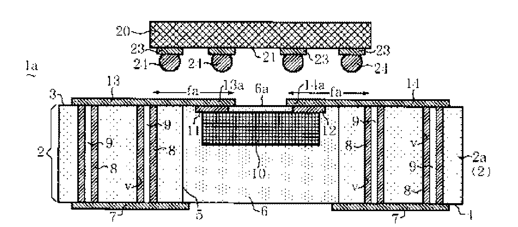
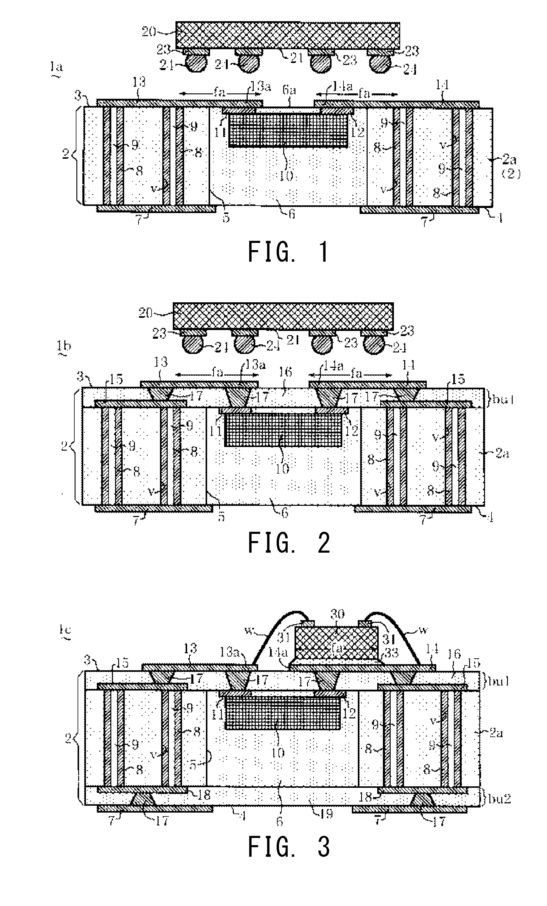
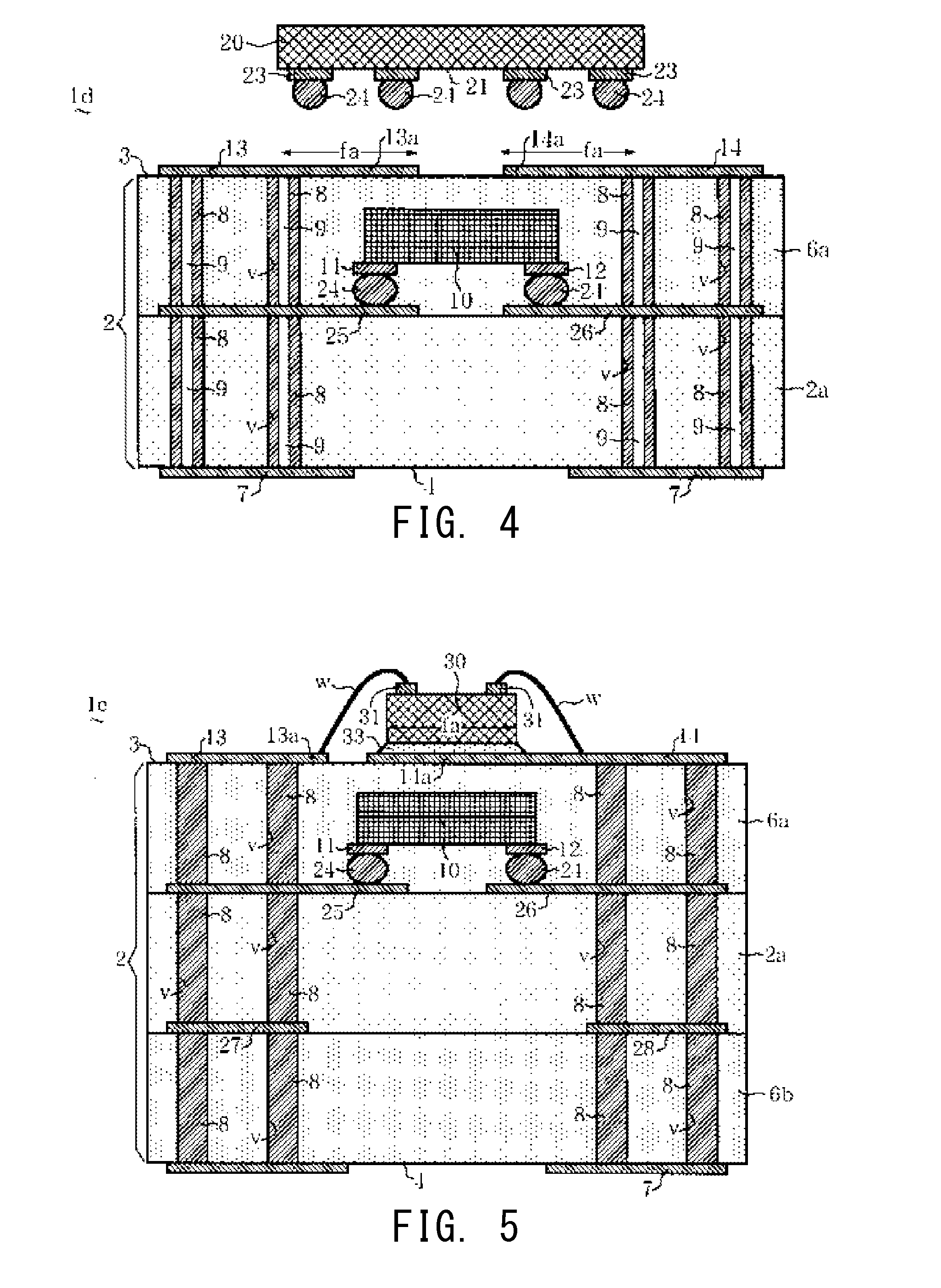
[0040]A mode for carrying out the invention will now be described. FIG. 1 is a vertical sectional view showing a light emitting element mounting wiring substrate 1a according to one embodiment of the present invention, and a light emitting diode (light emitting element) 20 to be mounted thereon.

[0041]As shown in FIG. 1, the light emitting element mounting wiring substrate 1a includes a substrate main body 2 having a front surface 3 and a back surface 4 and having a platelike shape as a whole; a pair of (a plurality of) element terminals 13, 14 formed on the front surface 3 of the substrate main body 2; a pair of outer connection terminals 7 formed on the back surface 4 of the substrate main body 2; and a Zener diode (an embedded component) 10 embedded in the substrate main body 2.

[0042]The substrate main body 2 is a core substrate (electrically insulating substrate) 2a formed of a hard resin or a ceramic material and having a thickness of about 30 μm to 1000 μm. An example of the ha...


PUM


Abstract

To provide a light emitting element mounting wiring substrate having a light emitting element mounting section on a substrate main body having a front surface and a back surface, and a confined component electrically connected to the light emitting element, such that the confine component does not obstruct the optical path of the light emitted from the light emitting element, resulting in uniform distribution of light intensity. The light emitting element mounting wiring substrate (1a) includes a substrate main body (2) which has a front surface (3) and a back surface (4) and which includes at least an insulating substrate (2a), and a plurality of element terminals (13, 14) formed on the front surface (3) of the substrate main body (2), at least one of the element terminals having a light emitting element mounting section (fa) on the top surface thereof, wherein the wiring substrate has a Zener diode (confined element) (10) embedded in the substrate main body (2), which element is electrically connected to a light emitting element (20) mounted on the mounting section (fa) and prevents application of overvoltage to the light emitting element (20).

Description

TECHNICAL FIELD[0001]The present invention relates to a wiring substrate having a substrate main body in which a light emitting element is to be mounted on a surface of the substrate main body.BACKGROUND ART[0002]There has been proposed a package for accommodating a light emitting element, the package having an insulating substrate which includes a mounting section for a light emitting element such as a light emitting diode, a mounting section for a protective element for preventing application of overvoltage to the light emitting element, and a wiring conductor for connecting the two elements; and a reflecting member which is attached to the front surface (a main surface) of the insulating substrate, which has a light-reflecting inner surface, and which surrounds the mounting section for a light emitting element. The protective element mounting section is disposed in a concavity of the insulating substrate capable of accommodating the protective element, and the concavity is define...

Claims


Application Information

Patent Timeline
Patent Type & Authority Applications(United States)
IPC IPC(8): H05K1/18
CPCH01L33/62H05K1/184H01L2224/48091H01L2224/48227H01L2224/73265H01L2224/32225H01L25/167H05K2201/10174H05K2201/10106H05K2201/0979H01L2924/30107H05K1/0257H05K1/185H05K3/4602H01L2924/00014H01L2924/00H05K3/00H05K3/46
Inventor NAGAI, MAKOTOKAWAGUCHI, KENZO
Owner NGK SPARK PLUG CO LTD
Why Eureka
Try Eureka