Electro-optical device and electronic apparatus

a technology of optical devices and electronic devices, applied in semiconductor devices, diodes, instruments, etc., can solve problems such as difficulty in writing from a data transfer line to a pixel, and achieve the effect of preventing the application of light to the transistor and high image quality

Active Publication Date: 2017-08-17
SEIKO EPSON CORP
View PDF1 Cites 17 Cited by
  • Summary
  • Abstract
  • Description
  • Claims
  • Application Information

AI Technical Summary

Benefits of technology

[0024]Thus, the third conductive layer and the sixth conductive layer overlap each other so as to have no gap in the second direction in a plan view. Accordingly, the light from the light emitting layer is reliably blocked by the third conductive layer and the sixth conductive layer, and thus applying of the light to the transistor is prevented. As a result, a light emitting element stably drives without changing the characteristics of the transistor.
[0025]Next, according to another aspect of the embodiment, an electronic apparatus includes the electro-optical device according to the above-described aspects of the embodiment. Regarding such an electronic apparatus, there is an electronic apparatus which has high image quality and in which the electro-optical device including a light emitting element such as an OLED is provided, and thus no color shift occurs, the characteristics of the transistor occurring by light from the light emitting layer is not changed, and writing from the data transfer line to a pixel is reliably performed.

Problems solved by technology

Thus, in the color filter type electro-optical device, there is a problem that a portion of light emitted from an OLED of a certain subpixel is transmitted through a color filter of an adjacent subpixel, and thus color mixing occurs depending on an angle at which a screen is observed.
As a result, time to select each of the scanning lines in the one horizontal scanning period becomes shorter, and thus writing from a data transfer line to a pixel may be difficult.

Method used


Image

  • Electro-optical device and electronic apparatus
  • Electro-optical device and electronic apparatus
  • Electro-optical device and electronic apparatus

Examples


first exemplary embodiment

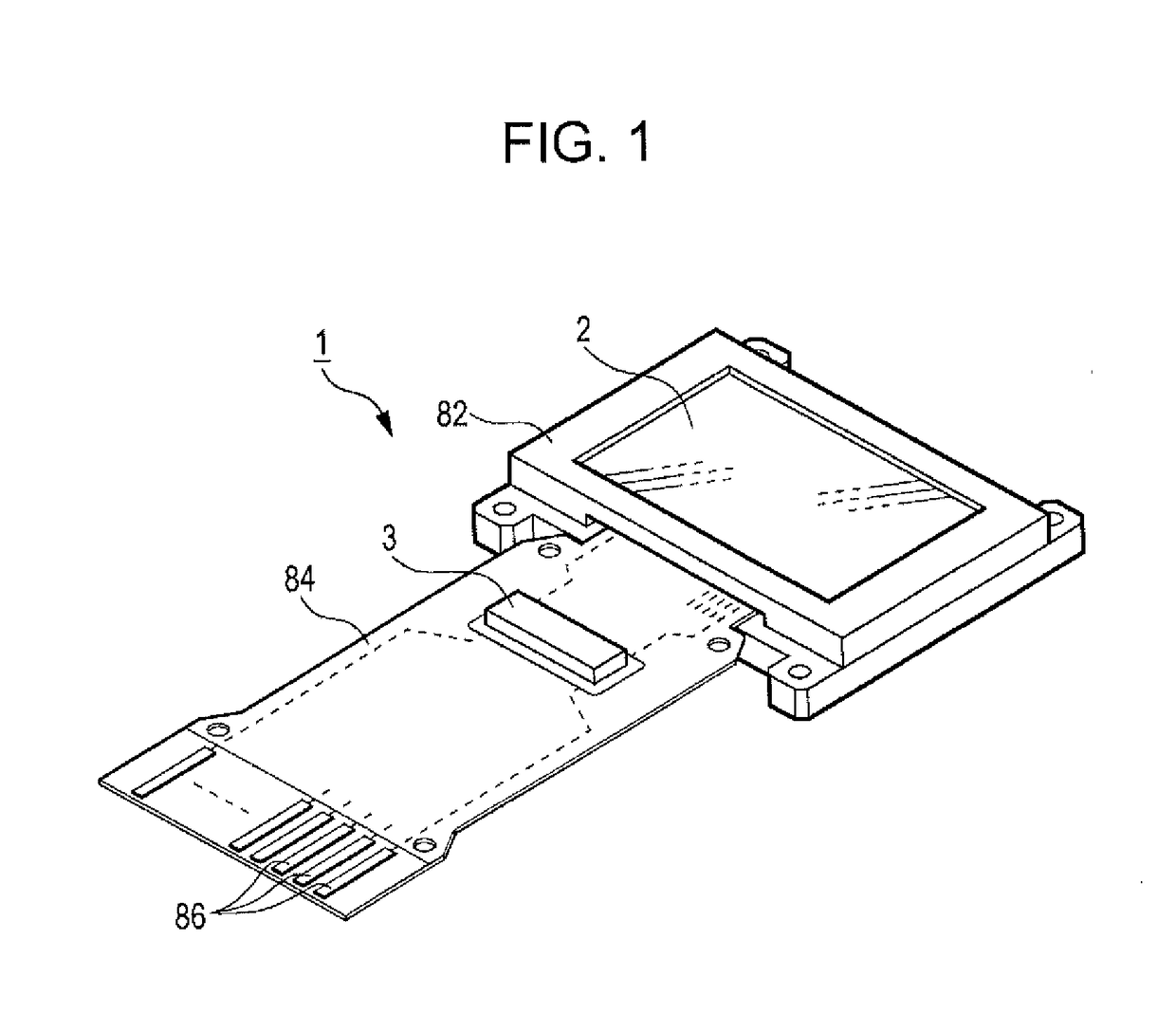
[0053]FIG. 1 is a perspective view illustrating a configuration of an electro-optical device 1 according to a first exemplary embodiment. The electro-optical device 1 is, for example, a micro-display which displays an image in a head mounted display.

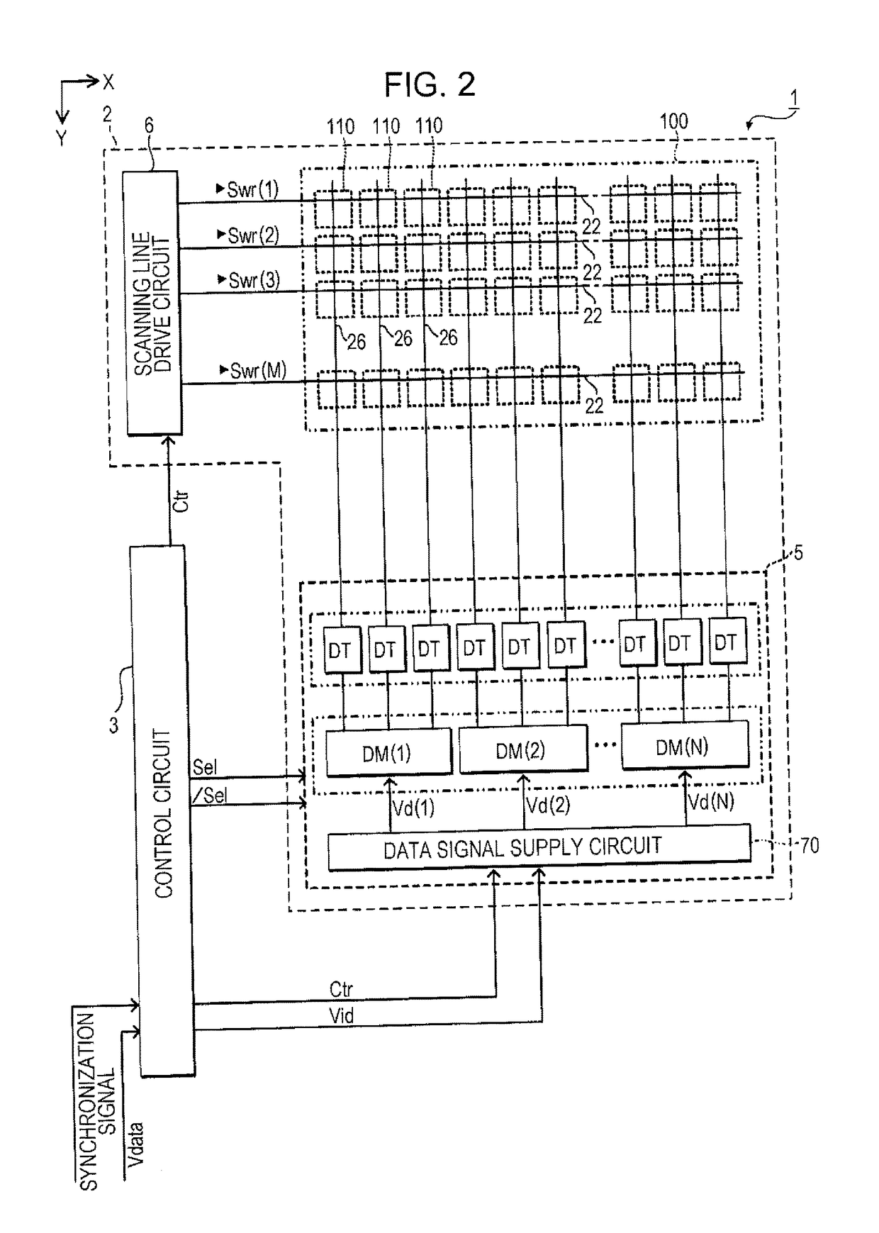
[0054]As illustrated in FIG. 1, the electro-optical device 1 includes a display panel 2, and a control circuit 3 for controlling an operation of the display panel 2. The display panel 2 includes a plurality of pixel circuits and a drive circuit for driving the pixel circuits. In the exemplary embodiment, the plurality of pixel circuits and the drive circuit provided in the display panel 2 are formed on a silicon substrate, and an OLED which is an example of a light emitting element is used as the pixel circuit. The display panel 2 is stored in, for example, a frame-like case 82 which is open in a display unit, and is connected to one end of a flexible printed circuit (FPC) substrate 84.

[0055]The control circuit 3 having a form of a semic...

second exemplary embodiment

[0138]Next, a second exemplary embodiment will be described with reference to FIGS. 13 to 22. FIG. 13 is a circuit diagram corresponding to FIG. 3 or 4 in the first exemplary embodiment.

[0139]A configuration in which the pixel circuit 110 includes four transistors is described in the first exemplary embodiment. However, in this exemplary embodiment, the pixel circuit 110 includes five transistors. In this exemplary embodiment, the data transfer line includes a first data transfer line and a second data transfer line.

[0140]The pixel circuit 110 in this exemplary embodiment will be described with reference to FIG. 13. As illustrated in FIG. 13, a first electrode 133-1 of a transfer capacitance 133 and a second electrode 134-2 of a shield capacitance 134 are electrically connected to a first data transfer line 26-1.

[0141]The second electrode 133-2 of the transfer capacitance 133, and the source or the drain of an initialization transistor Tfix are electrically connected to a second dat...

modification example

[0248]The embodiment is not limited to the above-described exemplary embodiments. For example, various modifications as will be described below can be made. The exemplary embodiments and modification examples may be appropriately combined.

[0249](1) In the above-described exemplary embodiments, a configuration in which the optical path adjusting layer is provided between the reflective layer and the pixel electrode is described. However, the embodiment is not limited to this configuration. The optical path adjusting layer may be omitted, and a pixel electrode having reflexibility may be used. In this case, the third conductive layer may be obtained by integrally forming the reflective layer and the pixel electrode.

[0250](2) In the above-described exemplary embodiments, a configuration in which a sealing film and the color filter are stacked on an OLED is described. However, the embodiment is not limited to this configuration. The color filter may be provided on a counter substrate.

[0...


PUM


Abstract

Subpixels of R, G, and B corresponding to a scanning line as a first conductive layer extended in a row direction and a data transfer line as a second conductive layer extended in a column direction are provided. A plurality of transistors in the subpixel of each of the colors is disposed along the column direction, and a reflective layer in the subpixel of at least one color is disposed along the row direction so as to overlap any transistor of subpixels of each display color. A center position of a disposition region of a reflective layer in one pixel unit including the subpixels of R, G, and B is different from a center position of a disposition region of a transistor in one pixel unit.

Description

BACKGROUND[0001]1. Technical Field[0002]The present disclosure relates to an electro-optical device and an electronic apparatus.[0003]2. Related Art[0004]Recently, an electro-optical device which uses an organic light emitting diode (OLED) as a light emitting element has been used in an electronic apparatus which can form a virtual image, such as a head mounted display. In such an electro-optical device, as disclosed in JP-A-2013-211147, a technology using a color filter is proposed as one of technologies which realize color display.[0005]In this technology, emitted light beams of red color, green color, and blue color are obtained through color filters of three primary colors, that is, red, green, and blue, by using an OLED which emits white light as a light source. A combination of an OLED and a filter for any color of the three primary colors is assumed to be a subpixel, and a combination of subpixels of the three primary colors is assumed to be a pixel. Such pixels are arranged ...

Claims


Application Information

Patent Timeline
Patent Type & Authority Applications(United States)
IPC IPC(8): H01L27/32H01L51/52
CPCH01L27/3262H01L51/5265H01L27/3276H01L27/322H01L51/5271H01L27/3265H01L27/1214H01L27/3206H10K59/121H10K59/1213H10K50/856G09G3/325G09G2300/0842G09G2300/0861H10K59/30H10K59/38H10K59/1216H10K59/126H10K59/131H10K50/852G09G3/32
Inventor KOSHIHARA, TAKESHIOTA, HITOSHINOZAWA, RYOICHI
Owner SEIKO EPSON CORP
Why Eureka
Try Eureka