Position adjustable probing device and probe card assembly using the same

Active Publication Date: 2014-10-16
MICROELECTRONICS TECH INC
View PDF6 Cites 14 Cited by
  • Summary
  • Abstract
  • Description
  • Claims
  • Application Information

AI Technical Summary

Benefits of technology

[0009]The present invention has been accomplished in view of the above-noted circumstances. It is an objective of the present invention to provide a position adjustable probing device having an elevation adjusting s

Problems solved by technology

It is found that the probe head 10, space transforming substrate 11, or the circuit board 12 will be easily damaged due to the processing error or mistake in soldering.
However, performing desoldering process will have a great risk of damaging the circuit board 12, the space transforming substrate 11 or the probe head 10.
However, becau

Method used


Image

  • Position adjustable probing device and probe card assembly using the same
  • Position adjustable probing device and probe card assembly using the same
  • Position adjustable probing device and probe card assembly using the same

Examples


Example

[0035]The present invention is to disclose a position adjustable probing device for testing semiconductor chips or photoelectric components. Since the principle of use and basic function of the probe card are well known for a person skilled in the art, the detailed description thereof will not be positively recited thereunder for purpose of concise illustration. Further, it is to be understood that the drawings disclosed in the present invention are given by way of schematically illustrating the structural features of the present invention only; therefore, they are not, or need not to be, sketched according to actual dimension in detail.

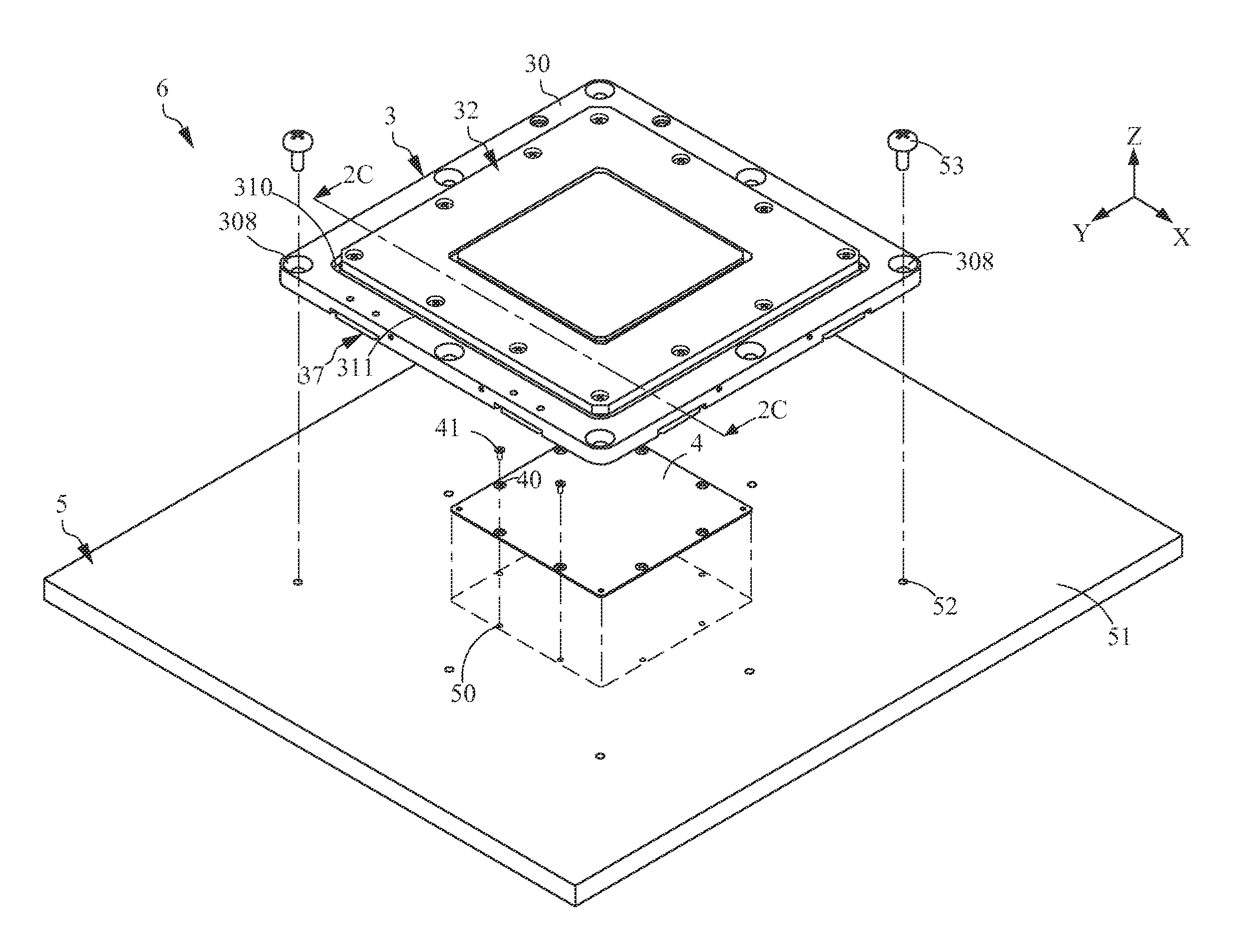
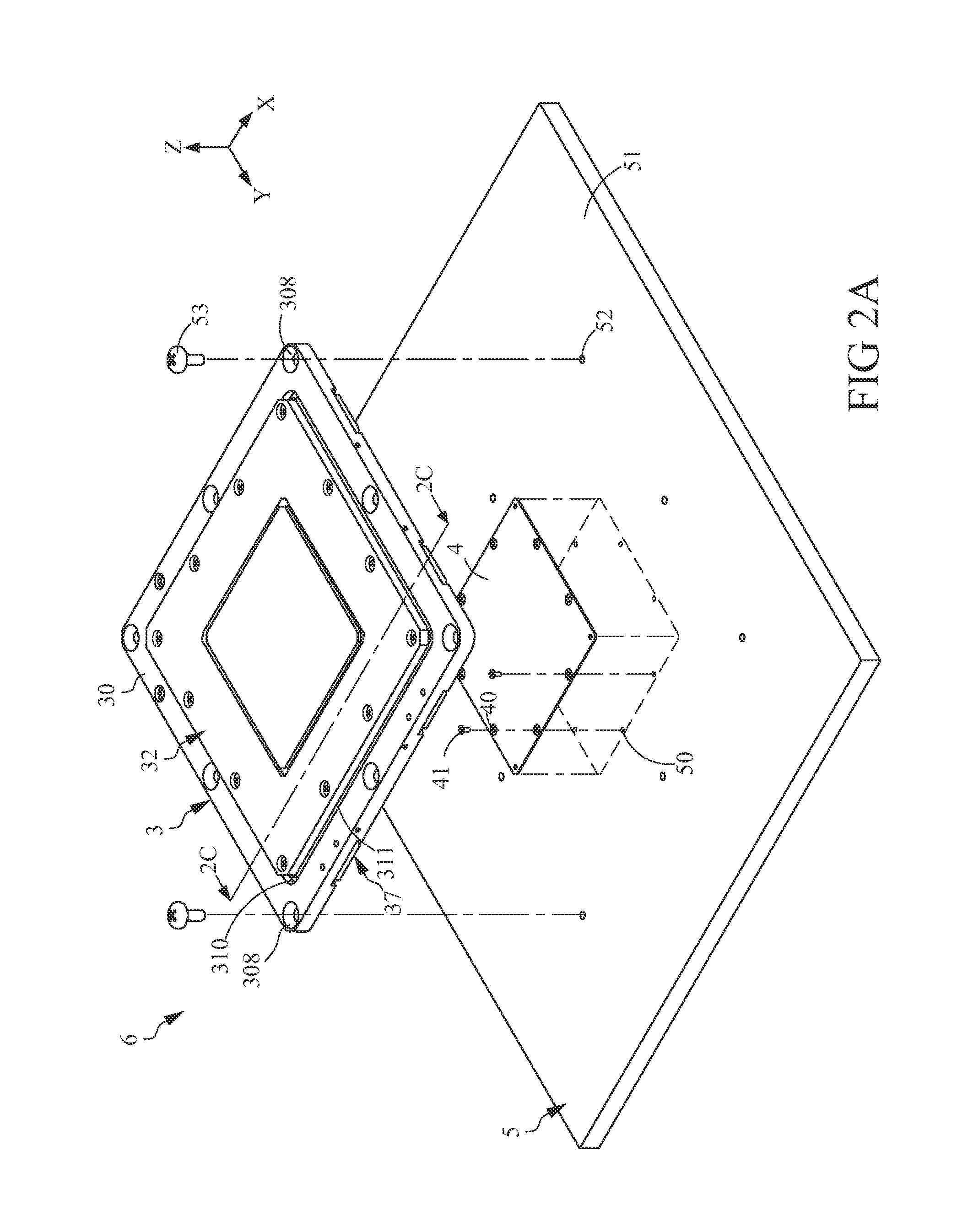
[0036]FIG. 2A shows a position adjustable probing device according to an embodiment of the present invention, FIG. 2B shows the position adjustable probing device of the embodiment of the present invention in an exploded manner, and FIG. 2C is a schematically sectional view of FIG. 2A. The probing device defined in the present invention indicates a p...


PUM


Abstract

A position adjustable probing device adapted for being mounted to a circuit board includes a frame, a probe head, a space transformer module and an elevation adjusting structure. The frame has a first surface, a second surface opposite to the first surface, and a first opening penetrating through the first and second surfaces. The probe head is coupled to the frame. The space transformer module is disposed in the first opening. The elevation adjusting structure is provided at the frame and has a plurality of spacers for adjusting a position of the frame relative to a reference surface in a vertical direction.

Description

CROSS-REFERENCE TO RELATED APPLICATIONS[0001]This application claims priorities from Taiwan Patent Application Nos. 102113400, 102206910 and 102206911 filed on Apr. 16, 2013 and Taiwan Patent Application No. 102214129 filed on Jul. 26, 2013, the entire contents of which are incorporated herein by reference.BACKGROUND OF THE INVENTION[0002]1. Field of the Invention[0003]The present invention relates generally to position adjusting mechanisms used in probe cards and more particularly, to a position adjustable probing device and a probe card assembly using the same.[0004]2. Description of the Related Art[0005]It is well-known that a device under test (hereinafter referred to as “DUT”), such as a die on a wafer, is indirectly contacted with a testing apparatus through a probe card. By means of signal transmission and analysis, electric characteristics of the DUT can be obtained. The conventional probe card generally comprises fine probe needles arranged in a desired manner that each pro...

Claims


Application Information

Patent Timeline
IPC IPC(8): G01R1/04
CPCG01R1/0408G01R31/2889G01R1/07378
Inventor CHEN, TSUNG-YILEE, CHUNG-TSECHEN, SHIH-SHIN
Owner MICROELECTRONICS TECH INC
Why Eureka
Try Eureka