Touch color filter and manufacturing method thereof and touch display panel

a technology of touch display panel and manufacturing method, which is applied in the direction of instruments, details of portable computers, coatings, etc., can solve the problems of color shift caused by transparent sensing patterns, high manufacturing cost, and high manufacturing complexity, and achieve the effect of reducing overall manufacturing cost and favorable view quality

Inactive Publication Date: 2014-10-23
CHUNGHWA PICTURE TUBES LTD
View PDF4 Cites 9 Cited by
  • Summary
  • Abstract
  • Description
  • Claims
  • Application Information

AI Technical Summary

Benefits of technology

[0013]In view of the above, the touch sensing layer and the black matrix layer of the touch display panel described herein are both located on the same substrate, and the boundary of the touch sensing layer is located within the boundary of the black matrix layer. Thereby, the touch display panel has favorable view quality. In addition, the manufacturing method of the touch display panel described herein requires a relatively few number of photomasks for forming the touch display panel, thus reducing the overall manufacturing costs.

Problems solved by technology

In the on-cell type touch panel, for instance, transparent sensing patterns that serve as the touch components are frequently formed on the outside of the display panel; therefore, during the operation of the on-cell type touch panel, issues of visibility of transparent sensing patterns, reflection caused by metal bridge, and color shift caused by the transparent sensing patterns often occur.
By contrast, in the in-cell type touch panel, for instance, when the touch components are formed on an active device array substrate, a number of photomasks are required, thus enhancing the complexity of the entire manufacturing process.
Moreover, noise interference is apt to occur between active devices and touch components, which further reduces the sensitivity of the touch panel.

Method used


Image

  • Touch color filter and manufacturing method thereof and touch display panel
  • Touch color filter and manufacturing method thereof and touch display panel
  • Touch color filter and manufacturing method thereof and touch display panel

Examples


Embodiment Construction

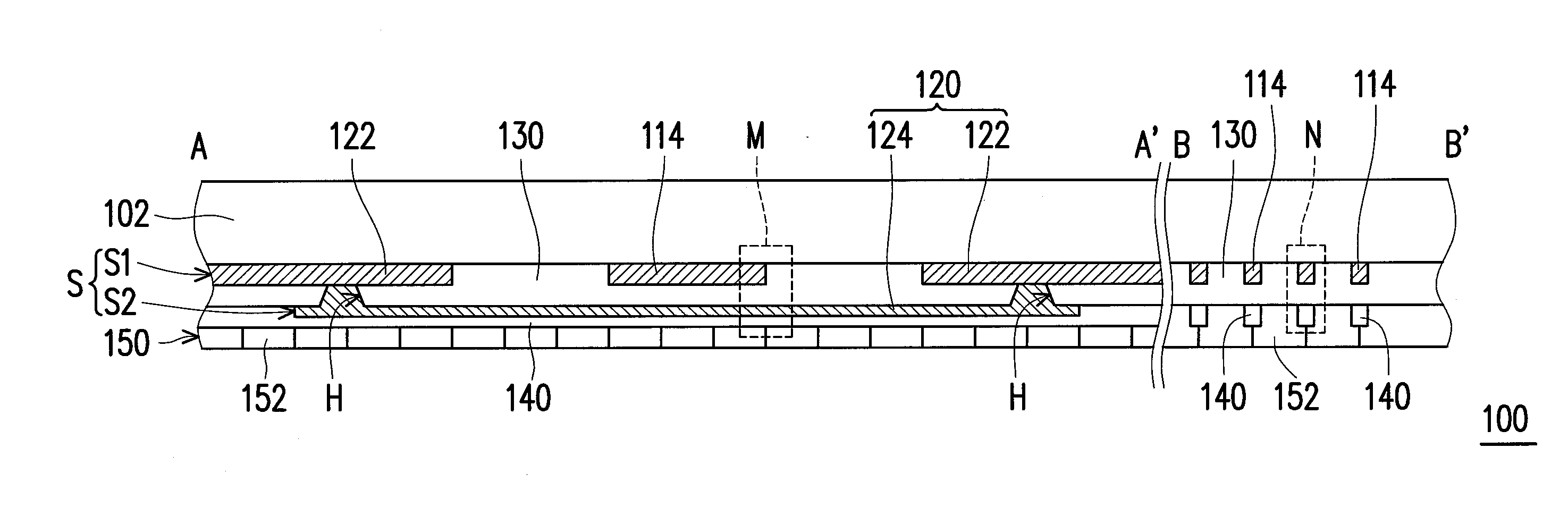
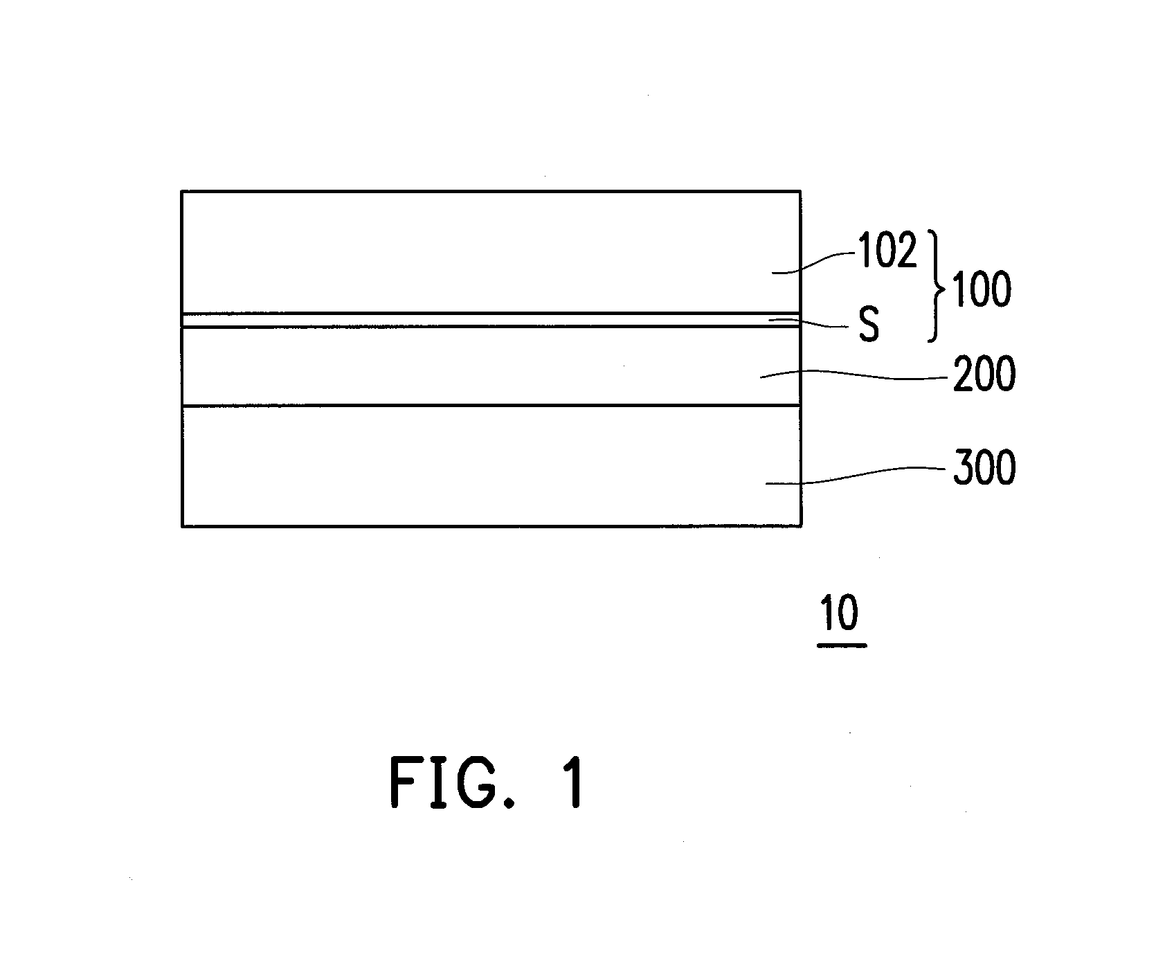
[0021]FIG. 1 is a schematic cross-sectional view illustrating a touch display panel according to an embodiment of the invention. With reference to FIG. 1, a touch display panel 10 includes a touch color filter 100, a light modulation layer 200, and an active device array substrate 300. The light modulation layer 200 is located between the touch color filter 100 and the active device array substrate 300. The touch color filter 100 includes a substrate 102 and a touch sensing layer S that is located on the substrate 102. The touch sensing layer S is located between the substrate 102 and the light modulation layer 200. The light modulation layer 200 is able to adjust the light passing through the light modulation layer 200 according to the display requirements. Here, the light modulation layer 200 is, for instance, a liquid crystal layer or an electrophoretic liquid layer, which should not be construed as a limitation to the invention. In other embodiments of the invention, the light m...


PUM


Abstract

A touch color filter includes a substrate, a touch sensing layer, a black matrix layer, and a color filter layer. The touch sensing layer is located on the substrate. The black matrix layer is located on the substrate. A boundary of the touch sensing layer is located within a boundary of the black matrix layer. The color filter layer is located on the substrate. The touch sensing layer and the black matrix layer are located between the substrate and the color filter layer, and the color filter layer covers the touch sensing layer and the black matrix layer.

Description

CROSS-REFERENCE TO RELATED APPLICATION[0001]This application claims the priority benefit of Taiwan application serial no. 102114196, filed on Apr. 22, 2013. The entirety of the above-mentioned patent application is hereby incorporated by reference herein and made a part of this specification.BACKGROUND OF THE INVENTION[0002]1. Field of the Invention[0003]The invention relates to a touch color filter, a manufacturing method thereof, and a touch display panel.[0004]2. Description of Related Art[0005]According to the way to arrange a touch panel and a display panel, the touch panel may be substantially categorized into an added-on type touch panel, an on-cell type touch panel, and an in-cell type touch panel. In the added-on type touch panel, touch components are often formed on a substrate to form a touch panel, and the touch panel is then adhered to an outer surface of a display panel. In the on-cell type touch panel, touch components are integrated onto a display panel. In the in-ce...

Claims


Application Information

Patent Timeline
Patent Type & Authority Applications(United States)
IPC IPC(8): G06F1/16
CPCG06F1/169G06F2203/04103G06F3/0412G06F3/041
Inventor CHANG, CHIU-PINGKUO, CHI-LIANGHSU, TSUNG-WEI
Owner CHUNGHWA PICTURE TUBES LTD
Why Eureka
Try Eureka