

Manufacturing method of silicon solar cell and silicon solar cell
a manufacturing method and solar cell technology, applied in the field of optoelectronic devices, can solve the problems of unstable eutectic layer formed in the opening, affecting the overall efficiency and yield of the solar cell, and achieve the effect of high conversion efficiency
Inactive Publication Date: 2014-10-30
TERASOLAR ENERGY MATERIALS CORP
View PDF0 Cites 8 Cited by
- Summary
- Abstract
- Description
- Claims
- Application Information
AI Technical Summary
Benefits of technology
[0009]The present invention provides a manufacturing method for a silicon solar cell, which offe
Problems solved by technology
However, if the parameters for removing the dielectric layer, e.g., depth, etc., are not properly controlled during the process of forming the opening in the dielectric
Method used
View moreImage
Smart ImageViewing Examples

Examples
 PUM
 Abstract
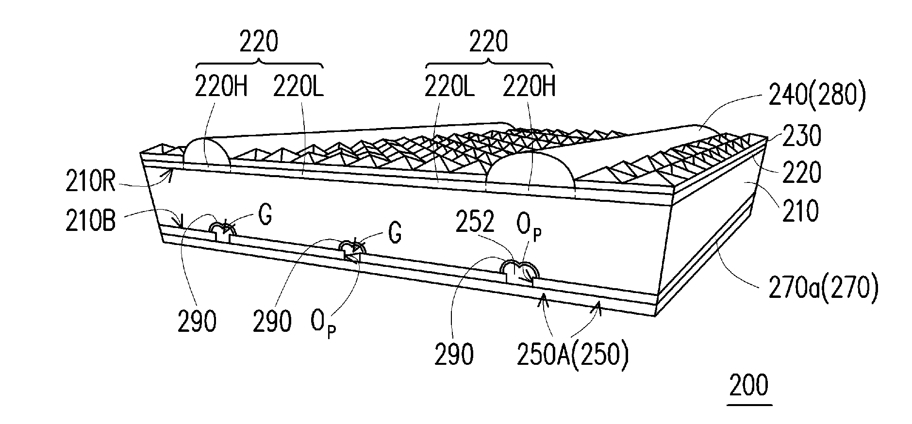
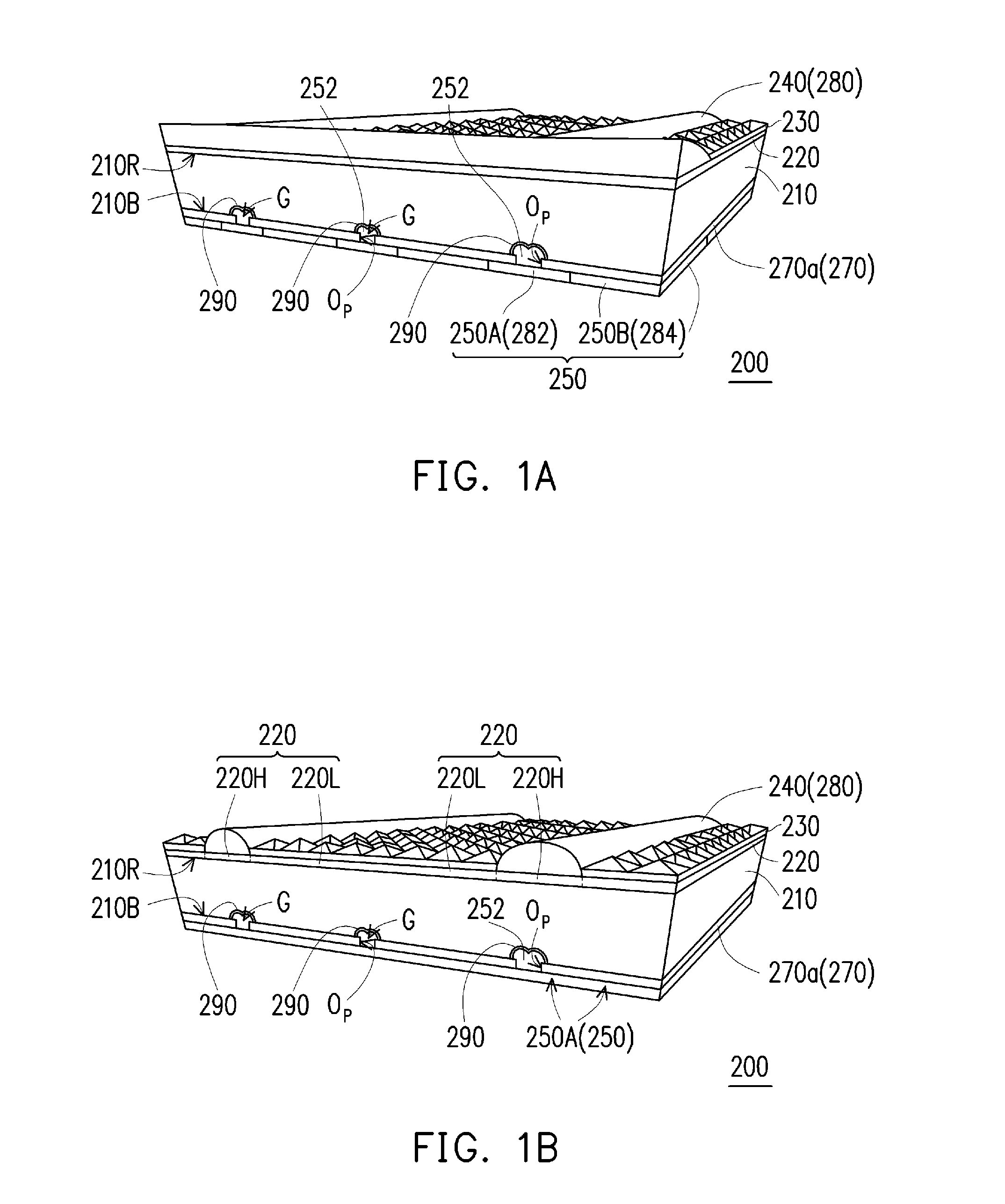
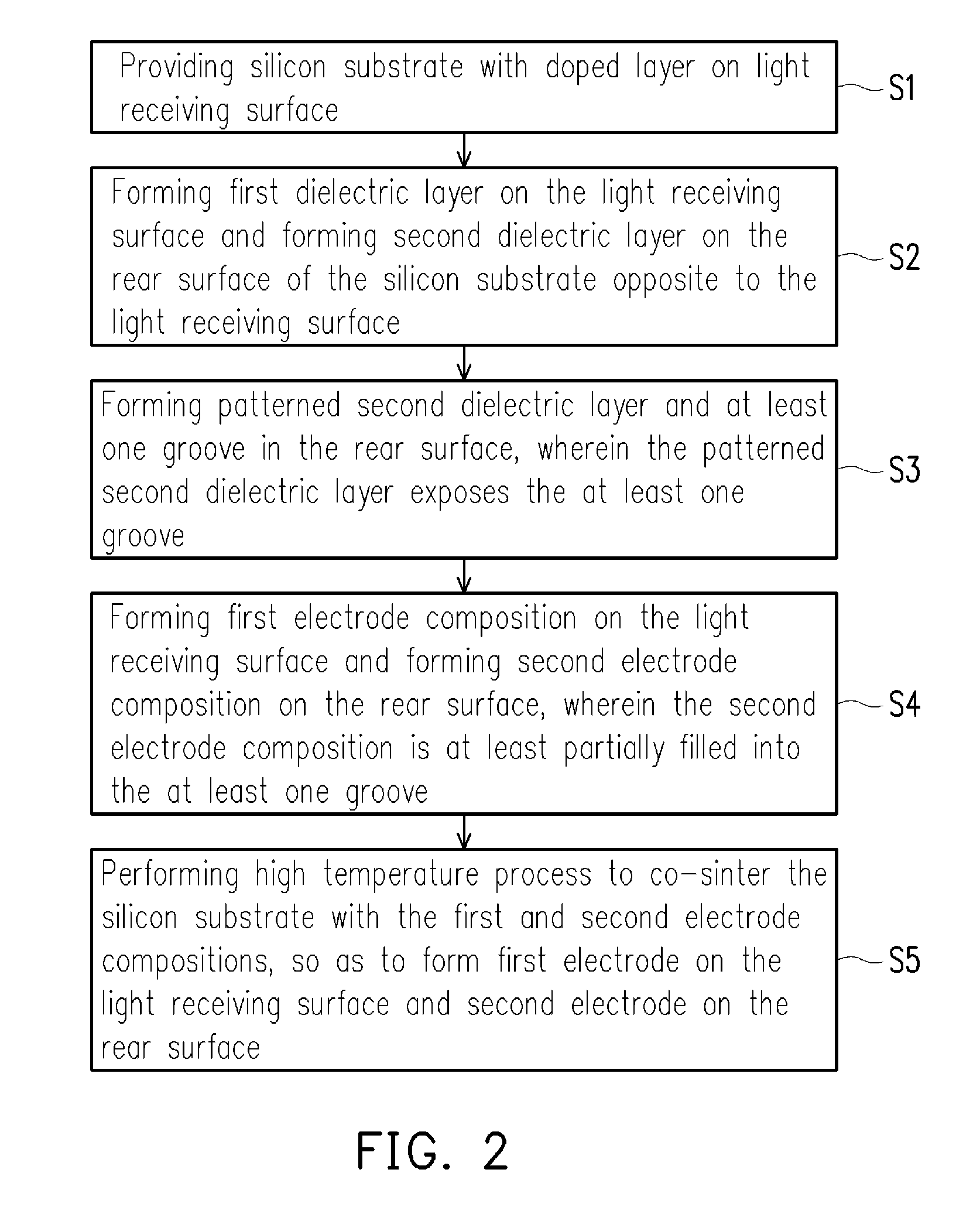
A manufacturing method of a silicon solar cell and the silicon solar cell thereof are provided. A silicon substrate formed with a doped layer on a light receiving surface thereof is provided. First and second dielectric layers are respectively formed on the light receiving surface and the rear surface of the silicon substrate. A patterned second dielectric layer with an opening and a groove in the silicon substrate are formed by partially removing the second dielectric layer and the silicon substrate. First and second electrode compositions are respectively formed on the light receiving surface and the rear surface, and the second electrode composition is filled into the groove. After performing a high temperature process to co-firing the silicon substrate and the first and second electrode compositions, a first electrode and a second electrode are respectively formed on the light receiving surface and the rear surface.
Description
CROSS-REFERENCE TO RELATED APPLICATION[0001]This application claims the priority benefit of Taiwan application serial no. 102115465, filed on Apr. 30, 2013. The entirety of the above-mentioned patent application is hereby incorporated by reference herein and made a part of this specification.BACKGROUND[0002]1. Field of the Present Disclosure[0003]The present invention relates to an optoelectronic device and the manufacturing method thereof. More particularly, the present invention relates to a manufacturing method of a silicon solar cell and a silicon solar cell.[0004]2. Description of Related Art[0005]As solar energy is a kind of unlimited and non-polluting energy, it has been highly expected as the substitute solution of current petrol energy which has long suffered from pollution and shortage problems. Solar cells can directly convert solar energy to electrical energy and has drawn more and more attentions these years.[0006]The solar cell is a photovoltaic device. The typical str...
Claims
Login to View More Application Information
Patent Timeline
 IPC IPC(8): H01L31/0236H01L31/0224H01L31/18
CPCH01L31/02366H01L31/1804H01L31/022425H01L31/02167Y02E10/547Y02E10/50
InventorCHOU, YI-CHINLIU, CHIA-YUNCHENG, CHENG-LIANGWANG, PIN-SHENGWU, BANG-HAO
OwnerTERASOLAR ENERGY MATERIALS CORP