
Circuitry configurable based on device orientation

Inactive Publication Date: 2014-11-13
OSRAM SYLVANIA INC
View PDF2 Cites 0 Cited by
  • Summary
  • Abstract
  • Description
  • Claims
  • Application Information

AI Technical Summary

Benefits of technology

The present invention relates to a method for placing electronic devices into circuitry, which can be configurable based on the orientation of the devices. This allows for the efficient placement of high volumes of devices into circuitry, reducing the time and cost of manufacturing. The invention uses a pick-and-place manufacturing process to place devices into circuitry, but the orientation of the devices can affect the efficiency of the process. The invention provides a solution to control the orientation of devices in the circuitry, allowing for better device placement. This can be useful, for example, in LED lighting where the devices need to be placed in a specific orientation to ensure proper functionality. The invention can be used in conjunction with fluidic self-assembly, which uses a liquid bath to place components in their desired locations. Overall, the invention improves the efficiency and speed of electronic assembly.

Problems solved by technology

While pick-n-place manufacturing can do the job, high machine time and upkeep costs, limited production speed, etc. for performing such simple / repetitive assembly can be prohibitive.
In particular, the wetting effect of the melted solder may cause conductive pads or bumps on the devices to be drawn to conductive pads in the device locations.
While FSA may provide a method by which circuitry may be populated with a large number of devices, at least one issue still exists in regard to device orientation in the circuitry.
Currently no effective provisions exist to control the orientation of devices being populated into the circuitry.
For example, existing control measures require custom devices and / or circuitry to mechanically steer device orientation, which may be prohibitive due to substantially increased material costs.

Method used


Image

  • Circuitry configurable based on device orientation
  • Circuitry configurable based on device orientation
  • Circuitry configurable based on device orientation

Examples


Embodiment Construction

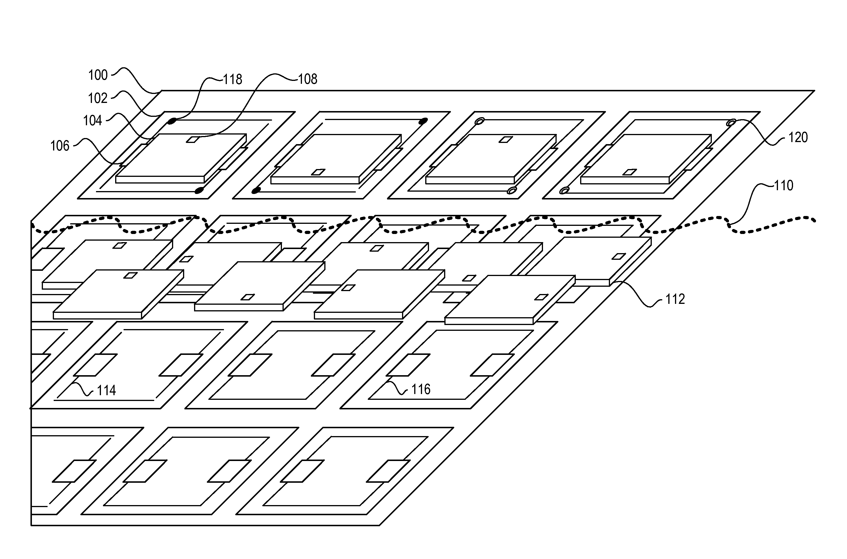
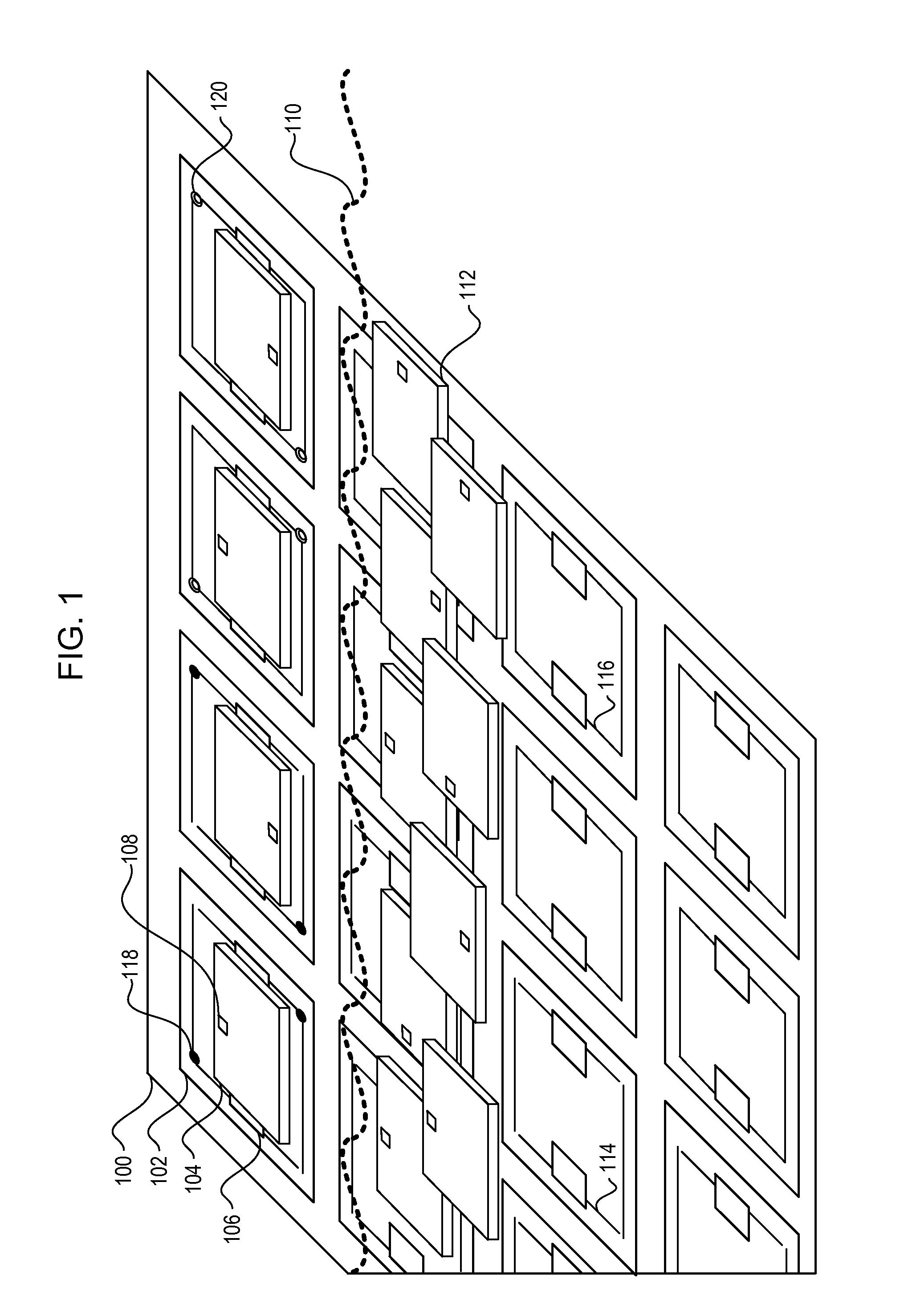
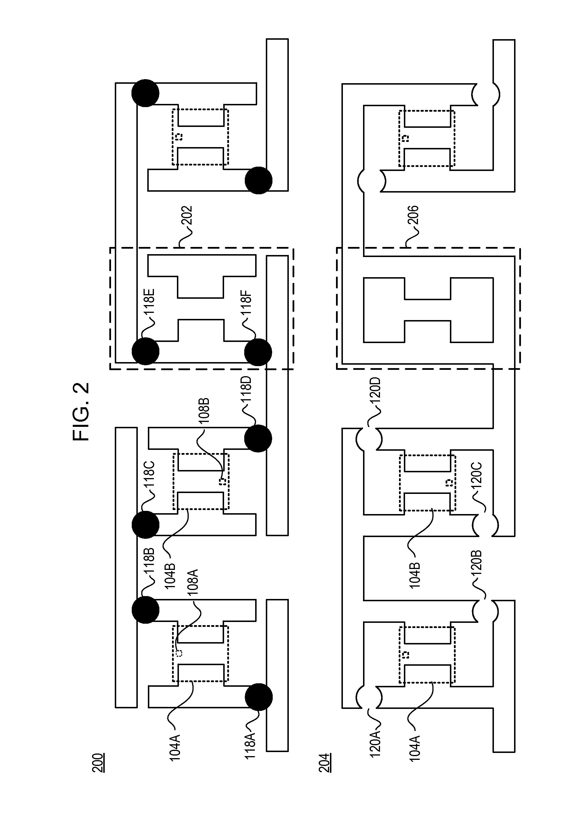
[0012]As referenced herein, “circuitry” may comprise any substrate onto which electronic devices may be inserted, placed, populated, etc. Examples of circuitry may include, but are not limited to, circuit boards, flexible substrates, packages such as multichip modules (MCM), etc. In general, circuitry may “configurable” consistent with embodiments of the present disclosure in that conductors in the circuitry may be configurable based on, for example, the orientation of devices populated into the circuitry. Configuring conductors may comprise, for example, adding conductive material to at least one conductor or removing at least part of at least one conductor. Adding conductive material may bridge a space existing between at least two sections of a conductor (e.g., to form a conductive path between the segments), and removing at least part of a conductor may be used to create an open circuit in a conductor (e.g., to stop conduction in the at least one conductor). For example, devices...


PUM


Abstract

The present disclosure is directed to circuitry configurable based on device orientation. Example circuitry may comprise at least one device location and configurable conductors. The at least one device location may include at least two conductive pads onto which a device may be populated by a manufacturing process. The configurable conductors may be coupled to each of the at least two conductive pads. The configurable conductors may be configured by adding conductive material to at least one configurable conductor or subtracting at least part of at least one configurable conductor. For example, conductive material may be added to close a space between two segments of a configurable conductor to form a conduction path. Alternatively, at least part of at least one of a plurality of configurable conductors coupled to a conductive pad may be subtracted (e.g., cut) to stop conduction in the at least one configurable conductor.

Description

TECHNICAL FIELD[0001]The present invention relates to electronic assembly, and more specifically, to the placement of devices into circuitry that may be configurable based on device orientation.BACKGROUND[0002]In a typical electronics manufacturing process, circuitry including, but not limited to, printed circuit boards, flexible substrates, packages such as multichip modules (MCM), etc. may be populated with electronic devices using pick-and-place operations. For example, the circuitry may be routed through machines equipped with vision systems for identifying device placement locations in the circuitry and manipulators configured to pick up devices from a supply location (e.g., rail, reel, etc.) and place the devices into the previously identified device locations. Pick-and-place manufacturing has been effective at least from the standpoint of accurately populating circuitry with a variety of devices at a speed substantially faster than manual device insertion.[0003]However, appli...

Claims


Application Information

Patent Timeline
IPC IPC(8): H01L33/62H01L27/15
CPCH01L33/62H01L27/15H01L21/485H01L23/5382H01L24/95H01L25/0753H01L25/50H01L2224/16225H01L2224/95085H01L2224/95101H01L2224/95146H01L2924/12042H01L2924/12041G06F30/30G06F30/39G06F2115/06H01L2924/00G06F2119/18
Inventor SERRE, JEFFERY J.
Owner OSRAM SYLVANIA INC
Features
  • Generate Ideas
  • Intellectual Property
  • Life Sciences
  • Materials
  • Tech Scout
  • Unparalleled Data Quality
  • Higher Quality Content
  • 60% Fewer Hallucinations
Learn More