Passive detection of unauthorized electronic devices using wafer scale beam forming
a technology of electronic devices and wafer scale, applied in the field of radar imaging systems, can solve problems such as unauthorized electronic devices
- Summary
- Abstract
- Description
- Claims
- Application Information
AI Technical Summary
Benefits of technology
Problems solved by technology
Method used
Image
Examples
Embodiment Construction
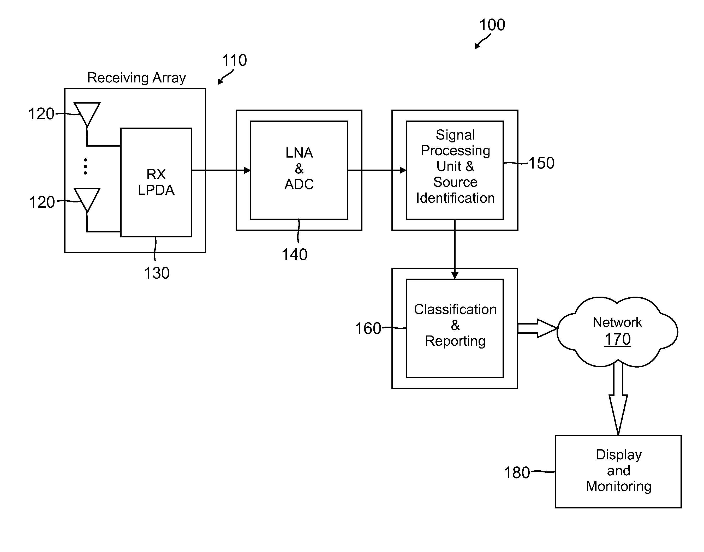
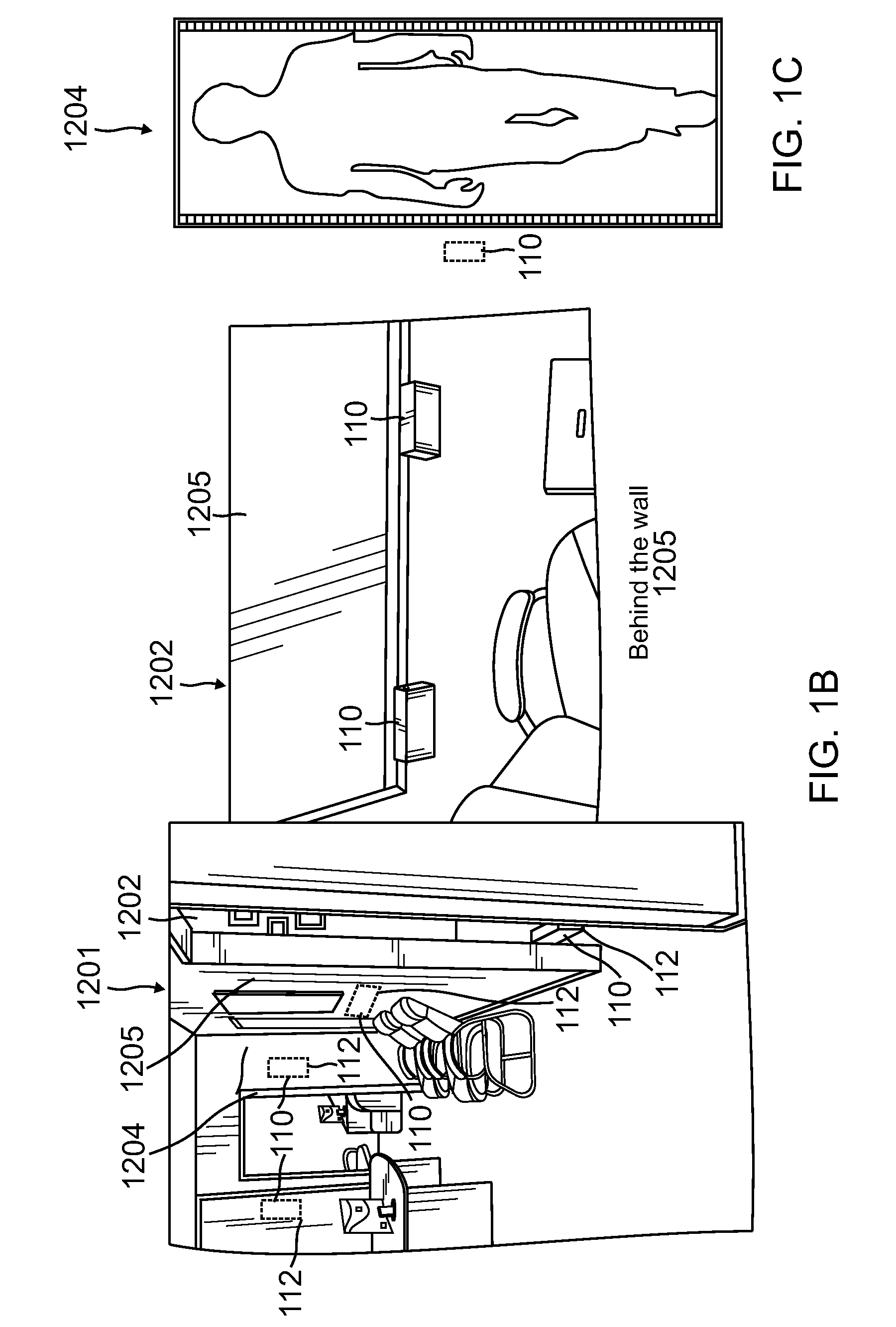
[0016]Methods and systems are disclosed that address the need for detecting and monitoring electronics systems not authorized to be used in secure areas. In one or more embodiments, by focusing a very narrow beam width antenna array, individuals can be screened who may have concealed electronics devices that can pose danger to the surroundings. One or more embodiments may implement a system for screening, where the subject walks through or in front of a passive detector (or scanning unit) to be screened for possession of unauthorized electronics devices. There is no need for removing clothing or accessories such as a jacket or backpack, for example.
[0017]In one embodiment, passive array electronic device sensors can be placed as a chain of sensors embedded inside construction of a building, or otherwise covertly placed, encompassing sensitive areas in such a way that tracking a person with an unauthorized electronic device may be enabled. A screening system according to one or more ...
PUM
 Abstract
Description
Claims
Application Information


