Radiation hardened circuit

a technology of hardening circuits and circuit elements, applied in the direction of pulse automatic control, reliability increasing modifications, instruments, etc., can solve the problems of parasitic currents in the integrated circuit, and it is not practicable to harden each circuit element using the known techniques abov

Inactive Publication Date: 2014-11-20
STMICROELECTRONICS (CROLLES 2) SAS +1
View PDF5 Cites 5 Cited by
  • Summary
  • Abstract
  • Description
  • Claims
  • Application Information

AI Technical Summary

Benefits of technology

[0023]According to another embodiment, there is provided a method of protecting first input circuitry of a data storage element from radiation comprising: generating, by the first input circuitry including a first plurality of components, a first input signal as a function of an initial signal; generating, by second input circuitry including a second plurality of components, a second input signal as a function of said initial signal, the second input circuitry being functionally equivalent to the first input circuitry; and wherein a voltage state stored by a first storage node of said data storage element is protected from a change in only one of said first and second input signals by being determined by the conduction state of a first transistor coupled to the first storage node and controlled based on said first input signal and of a second transistor coupled to the first storage node and controlled based on said second input signal.
[0024]According to another embodiment...

Problems solved by technology

Integrated circuits are generally sensitive to ionizing particles, which can induce parasitic currents in the integrated circuit.
However, for certain circuits, su...

Method used


Image

  • Radiation hardened circuit
  • Radiation hardened circuit
  • Radiation hardened circuit

Examples


Embodiment Construction

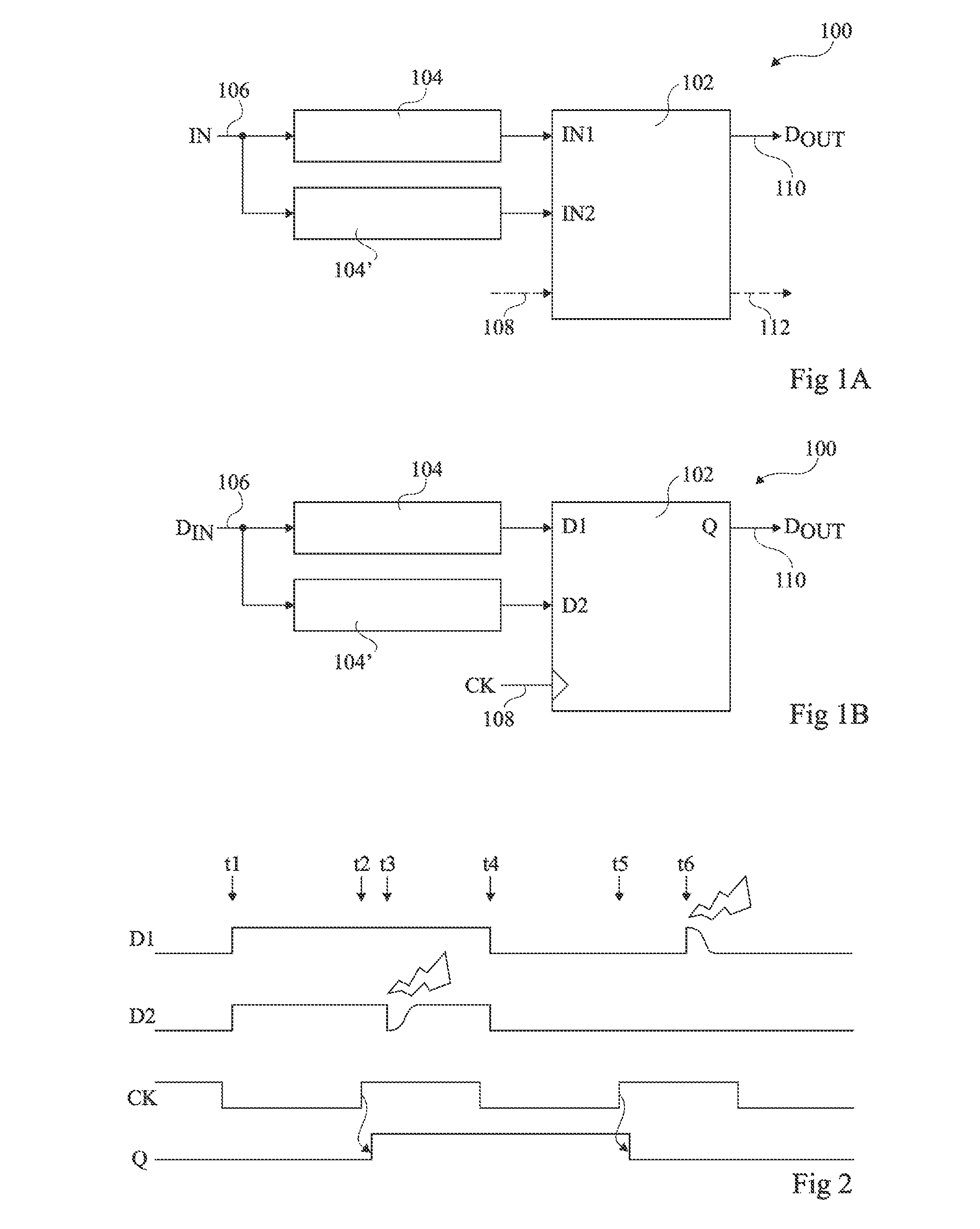
[0039]FIG. 1A illustrates a radiation hardened circuit 100 comprising a circuit block 102 having inputs IN1 and IN2.

[0040]The data input IN1 is coupled to and driven by input circuitry 104, which receives an input signal IN on a line 106. The input circuitry 104 comprises a plurality of components, for example logic components and / or analog components, that generates the signal at input IN1 as a function of the input signal IN. According to one example, the input circuitry 104 comprises combinational components, such as data buffers or other logic gates and not sequential logic. According to another example, the input circuitry 104 additionally or alternatively comprises one or more analog circuit components such as resistors, capacitors, inductors, transmission lines, etc. In any case, the input circuitry 104 for example does not store data from one clock cycle to the next.

[0041]The data input IN2 is coupled to and driven by input circuitry 104′, which is, for example, an identical...


PUM


Abstract

A circuit including a data storage element; first and second input circuitry coupled respectively to first and second inputs of the data storage element and each including a plurality of components adapted to generate, as a function of an initial signal, first and second input signals respectively provided to the first and second inputs; wherein the data storage element includes a first storage node and is configured such that a voltage state stored at the first storage node is protected from a change in only one of the first and second input signals by being determined by the conduction state of a first transistor coupled to the first storage node and controlled based on the first input signal and by the conduction state of a second transistor coupled to the first storage node and controlled based on the second input signal.

Description

CROSS REFERENCE TO RELATED APPLICATIONS[0001]This application claims the priority benefit of European Patent Application No. 13305644.0, filed May 17, 2013, and which application is hereby incorporated by reference to the maximum extent allowable by law.BACKGROUND[0002]This application claims the priority benefit of European Patent application number 13305644.0, filed on May 17, 2013, entitled “Radiation hardened circuit”, the content of which is hereby incorporated by reference in its entirety to the maximum extent allowable by law.[0003]1. Technical Field[0004]The present disclosure relates to a radiation hardened circuit and to a method of protecting a circuit from radiation.[0005]2. Discussion of the Related Art[0006]Integrated circuits are generally sensitive to ionizing particles, which can induce parasitic currents in the integrated circuit. In certain cases, these parasitic currents can be enough to flip the binary state of a data storage element in the circuit, such as a la...

Claims


Application Information

Patent Timeline
IPC IPC(8): H03K19/003H03L7/08
CPCH03L7/08H03K19/0033G11C5/005H03K3/0375H03L7/0896H03K3/356121H03L7/0891H03L7/095H03L7/18
Inventor GASIOT, GILLESCLERC, SYLVAINYOUSUF, JUNAIDGLORIEUX, MAXIMILIEN
Owner STMICROELECTRONICS (CROLLES 2) SAS
Why Eureka
Try Eureka