Light exposure system and light exposure process

a light exposure system and light exposure technology, applied in the field of light exposure systems and light exposure processes, can solve the problems of increasing manufacturing costs, affecting the high cost of light exposure equipment in the light exposure system used in the psa technology, so as to improve the competitiveness of products, reduce the exact time of light exposure processes, and reduce manufacturing costs

Active Publication Date: 2014-12-18
INNOLUX CORP
View PDF3 Cites 5 Cited by
  • Summary
  • Abstract
  • Description
  • Claims
  • Application Information

AI Technical Summary

Benefits of technology

[0009]In view of the foregoing subject, an objective of the invention is to provide a light exposure system and a light exposure process so that the light exposure system can be used more effectively and the tact time of the light exposure process can be decreased to lower down the manufacturing cost and enhance the competitiveness of the product.
[0016]As mentioned above, in the light exposure system and light exposure process according to the invention, the assembly cell is given the light exposure process, and the assembly cell includes a first substrate, a second substrate and a liquid crystal disposed between the first and second substrates. Besides, at least one of two moving stages carries the assembly cell. The transmission device can move at least one of the moving stages carrying the assembly cell or the light source module so that the light source module can emit the light to the assembly cells to complete the light exposure process. Thereby, the light exposure system is not idled for waiting for the preparatory work such as cell replacement and alignment, electrode contact or application of electric field. Therefore, the light source module of the light exposure system can be used more effectively and adequately and thus the tact time of the light exposure process can be reduced. Furthermore, the manufacturing cost is lowered down and the competitiveness of the product is enhanced.
[0017]Besides, in one embodiment of the invention, by the light exposure system and process, the problem of bright and dark bands caused by the uneven illumination provided by the light emitting elements of the light source module can be diminished.

Problems solved by technology

The light exposure system used in the PSA technology takes the highest part of the cost of the light exposure equipment.
So, the light exposure system is not used effectively and adequately.
Thus, if the production capacity needs to be increased, it is necessary to establish more light exposure systems and space, but this will raise the manufacturing cost and lower down the competitiveness of the product.

Method used


Image

  • Light exposure system and light exposure process
  • Light exposure system and light exposure process
  • Light exposure system and light exposure process

Examples


Embodiment Construction

[0024]The present invention will be apparent from the following detailed description, which proceeds with reference to the accompanying drawings, wherein the same references relate to the same elements.

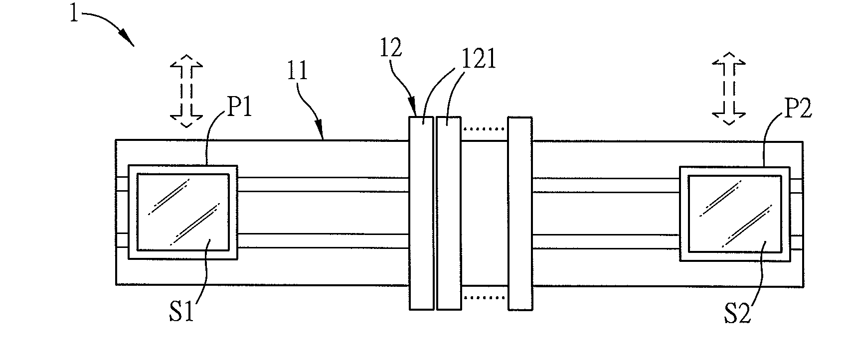
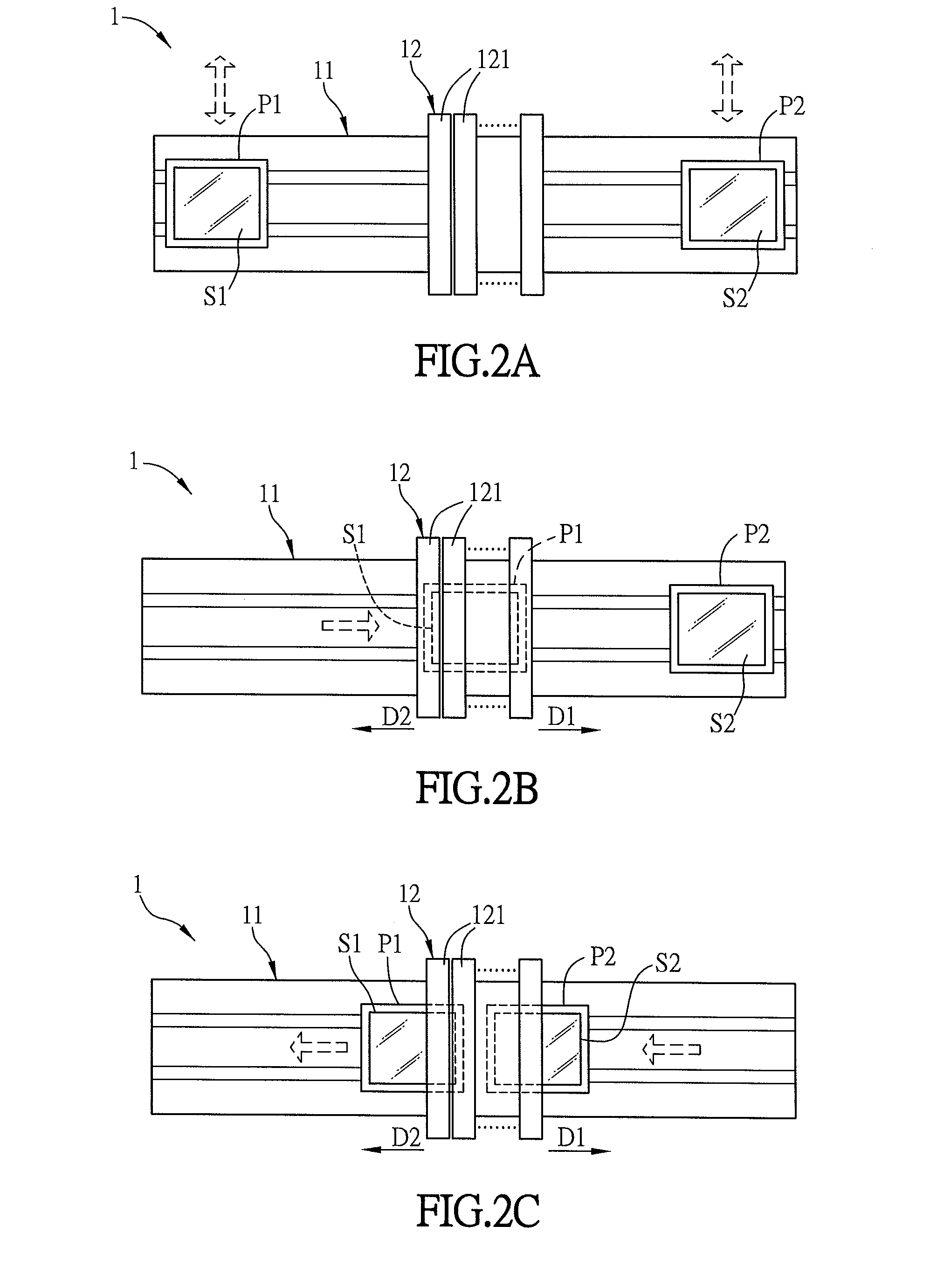
[0025]The light exposure system of the invention can be applied to the light exposure process of the in-plane switch (IPS) LCD apparatus, fringe field switching (FFS) LCD apparatus, vertical alignment mode (VA mode) LCD apparatus or 3D LCD apparatus. The type of the LCD apparatus is not limited in this invention.

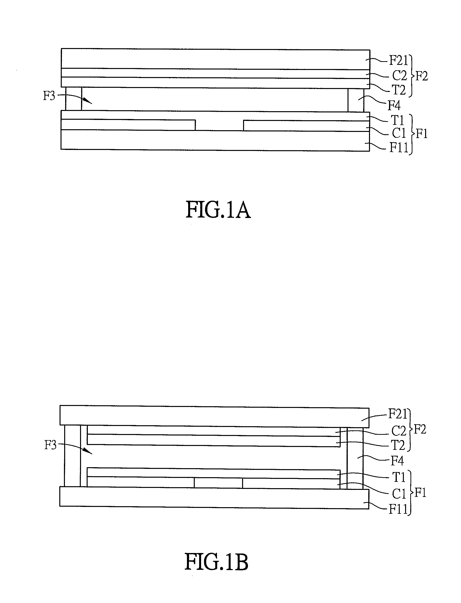
[0026]The light exposure system 1 according to the invention can execute a light exposure process to an assembly cell. The so-called assembly cell here includes, for example, a cell including an upper substrate, a lower substrate and a liquid crystal layer, but the cell has not been scribed yet. An assembly cell can include a display panel (including an upper substrate, a lower substrate and a liquid crystal layer) or include a plurality of display panels (including a pluralit...


PUM

PropertyMeasurementUnit
photosensitiveaaaaaaaaaa
electric fieldaaaaaaaaaa
transparent conductiveaaaaaaaaaa

Abstract

A light exposure system executes a light exposure process to an assembly cell, which includes a first substrate, a second substrate and a liquid crystal layer disposed between the first and second substrates. The light exposure system comprises a transmission device, two moving stages and a light source module. The moving stages are disposed on the transmission device and at least one of the moving stages carries the assembly cell. The light source module includes at least a light emitting element. The transmission device moves at least one of the moving stages carrying the assembly cell or the light source module and the light emitting element emits the light to the assembly cell. A light exposure process applied to the light exposure system is also disclosed.

Description

CROSS REFERENCE TO RELATED APPLICATIONS[0001]This Non-provisional application claims priority under 35 U.S.C. §119(a) on Patent Application No(s). 102121568 filed in Taiwan, Republic of China on Jun. 18, 2013, the entire contents of which are hereby incorporated by reference.BACKGROUND OF THE INVENTION[0002]1. Field of Invention[0003]The invention relates to a light exposure system and a light exposure process.[0004]2. Related Art[0005]With the progress of technologies, flat display devices have been widely applied to various kinds of fields. Especially, liquid crystal display (LCD) devices, having advantages such as compact structure, low power consumption, light weight and less radiation, gradually take the place of cathode ray tube (CRT) display devices and are widely applied to various electronic products, such as mobile phones, portable multimedia devices, notebooks, LCD TVs and LCD screens.[0006]In the multi-domain vertical alignment (MVA) process for enhancing the quality of ...

Claims


Application Information

Patent Timeline
Patent Type & Authority Applications(United States)
IPC IPC(8): G03F7/20
CPCG03F7/20G03F7/201
Inventor KAO, KER-YIHCHEN, TSAN-JENKAO, CHEN-KUANLEE, CHIEN-HSING
Owner INNOLUX CORP
Why Eureka
Try Eureka