

Display element
- Summary
- Abstract
- Description
- Claims
- Application Information
AI Technical Summary
Benefits of technology
Problems solved by technology
Method used
Image

Examples
first embodiment
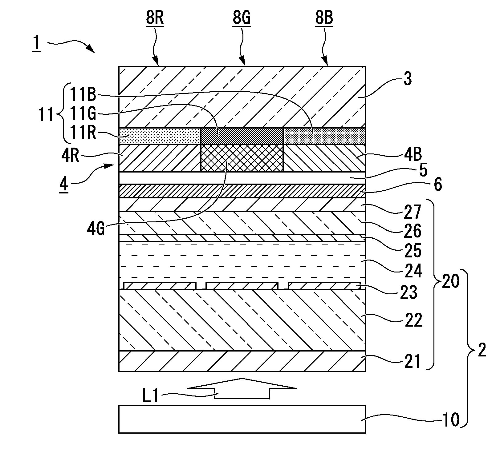
[0084](1) Entire Configuration of a Display Element
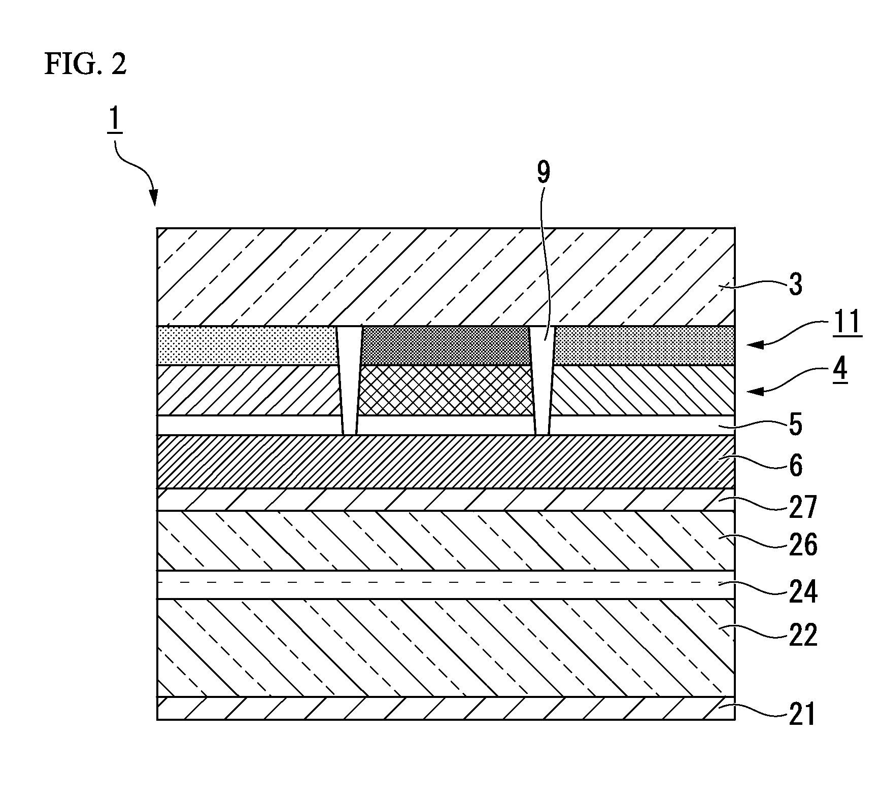
[0085]Hereinafter, a first embodiment will be described using FIGS. 1 to 7 and 13. FIG. 1 is a schematic cross-sectional view illustrating a display element of this embodiment, and FIG. 13 is a schematic cross-sectional view illustrating a display element of a comparative example.
[0086]The display element 1 of this embodiment includes an optical modulation portion 2, a substrate 3 arranged opposite to the optical modulation portion 2, a phosphor layer 4 arranged on the optical modulation portion 2 side of the substrate 3, a color filter layer 11 arranged between the substrate 3 and the phosphor layer 4, and a band pass filter 6 arranged with a low refractive index layer 5 interposed between the optical modulation portion 2 and the phosphor layer 4, as illustrated in FIG. 1. In the display element 1 of this embodiment, a red subpixel 8R that performs display by red light, a green subpixel 8G that performs display by green light, and ...
second embodiment
[0151]Hereinafter, a display element 1B of a second embodiment of the present invention will be described using FIGS. 8A and 8B.
[0152]A basic configuration of the display element 1B of this embodiment is the same as that of the display element 1 of the first embodiment, and the second embodiment is different from the first embodiment in that glass surfaces of an upper substrate 300 and a lower substrate 200 are directly bonded by a peripheral sealing material S2.
[0153]FIG. 8A is a schematic cross-sectional view illustrating a method of bonding primary portions of the display element 1B of this embodiment. FIG. 8B is a cross-sectional view illustrating a bonded configuration of the primary portions of the display element 1B of this embodiment. The same components in FIGS. 8A and 8B as those in FIG. 1 of the first embodiment are denoted with the same reference signs and a detailed description thereof is omitted.
[0154](1) Configuration of the Display Element
[0155]In the display element...
third embodiment
[0165]Hereinafter, a display element 1C of a third embodiment of the present invention will be described using FIG. 9.
[0166]A basic configuration of the display element 1C of this embodiment is the same as that of the display element 1 of the first embodiment, and the third embodiment is different from the first embodiment in that a low refractive index resin layer 12 is arranged between a phosphor layer 4 and a band pass filter 6 instead of the air layer.
[0167]FIG. 9 is a schematic cross-sectional view illustrating primary portions of the display element 1C of this embodiment. The same components in FIG. 9 as those in FIG. 1 of the first embodiment are denoted with the same reference signs and a detailed description thereof is omitted.
[0168]In the display element 1C of this embodiment, the low refractive index resin layer 12 is arranged between the phosphor layer 4 and the band pass filter 6, as illustrated in FIG. 9. For the low refractive index resin layer 12, for example, a poro...
PUM
 Abstract
Description
Claims
Application Information