Testing apparatus and method for microcircuit and wafer level IC testing

a technology for testing apparatus and circuit boards, applied in metal working apparatus, manufacturing tools, instruments, etc., can solve the problems of affecting the quality of the test results

Active Publication Date: 2015-01-15
JOHNSTECH INT
View PDF5 Cites 23 Cited by
  • Summary
  • Abstract
  • Description
  • Claims
  • Application Information

AI Technical Summary

Benefits of technology

[0045]d. forming an elastomeric block around probes between said upper and lower plates, and below said upstop;so that, said elastomer will drive said increased diameter toward said upper plate thereby providing a bias force on said probes toward said IC.

Problems solved by technology

As microcircuits continually evolve to be smaller and more complex, the test equipment that tests the microcircuits also evolves.
Mounting a defective microcircuit on a circuit board is relatively costly.
Once mounted on a circuit board, removing a microcircuit is problematic because the very act of melting the solder for a second time ruins the circuit board.
Thus, if the microcircuit is defective, the circuit board itself is probably ruined as well, meaning that the entire value added to the circuit board at that point is lost.
Each microcircuit must be tested in a way that identifies all defective devices, but yet does not improperly identify good devices as defective.
Either kind of error, if frequent, adds substantial overall cost to the circuit board manufacturing process, and can add retest costs for devices improperly identified as defective devices.
Microcircuit test equipment itself is quite complex.
Because of the small size of microcircuit probes and the spacing between them, even small errors in making the probe will result in incorrect connections.
Connections to the microcircuit that are misaligned or otherwise incorrect will cause the test equipment to identify the die under test (DUT) as defective, even though the reason for the failure is the defective electrical connection between the test equipment and the DUT rather than defects in the DUT itself.
A further problem in microcircuit test equipment arises in automated testing.
The sheer number of tests cause wear on the tester pins making electrical connections to the microcircuit terminals during testing.
This wear dislodges conductive debris from both the tester pins and the DUT terminals that contaminates the testing equipment and the DUTs themselves.
The debris eventually results in poor electrical connections during testing and false indications that the DUT is defective.
The debris adhering to the microcircuits may result in faulty assembly unless the debris is removed from the microcircuits.
Removing debris adds cost and introduces another source of defects in the microcircuits themselves.
If the test equipment is off line for extended periods of normal maintenance, the cost of testing an individual microcircuit increases.
In general, it is impractical to solder and remove each electrical terminal on the microcircuit being contacted by a corresponding electrical probe on the tested.
First, in making the temporary contact with the ball terminals, the tester should not damage the S&P terminal surfaces that contact the circuit board, since such damage may affect the reliability of the solder joint for that terminal.
Tin-based solder alloys are likely to develop an oxide film on the outer surface that conducts poorly.

Method used


Image

  • Testing apparatus and method for microcircuit and wafer level IC testing
  • Testing apparatus and method for microcircuit and wafer level IC testing
  • Testing apparatus and method for microcircuit and wafer level IC testing

Examples


Embodiment Construction

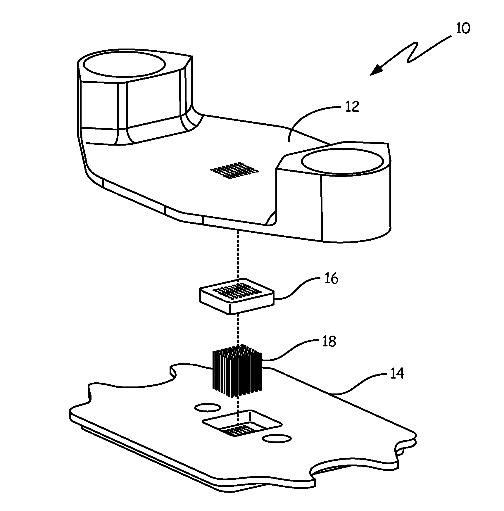
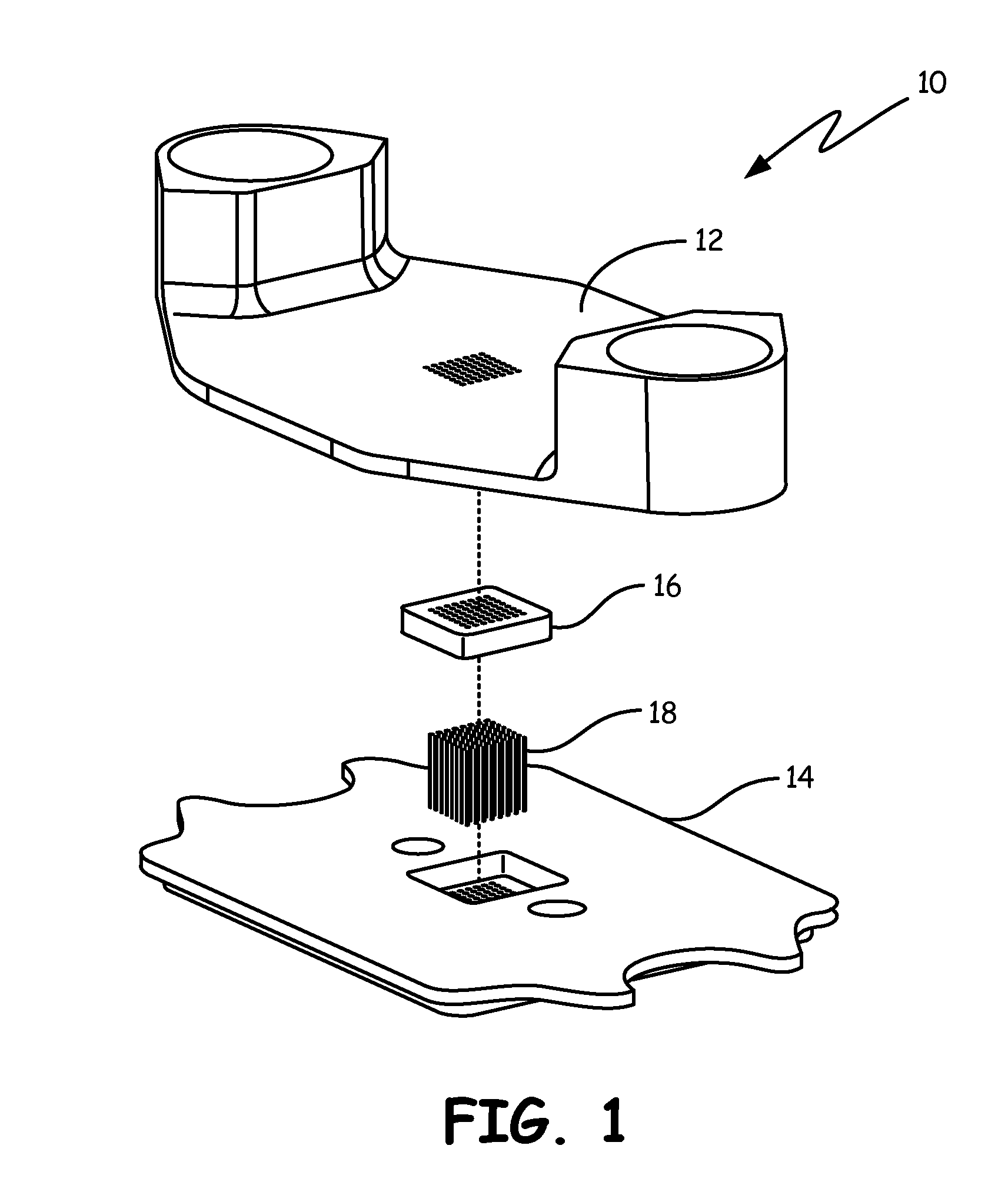
[0091]Consider an electrical chip, i.e. an integrated circuit that is manufactured to be incorporated into a larger system. When in use, the chip electrically connects the device to the larger system by a series of pins or terminals. For instance, the pins on the electrical chip may plug into corresponding sockets in a computer, so that the computer circuitry may electrically connect with the chip circuitry in a predetermined manner. An example of such a chip may be a memory card or processor for a computer, each of which may be insertable into a particular slot or socket that makes one or more electrical connections with the chip.

[0092]It is highly desirable to test these chips before they are shipped, or before they are installed into other systems. It is even more desirable to test the chips while they are still on the wafer from which they were formed. Such chips are called dice or an individual die, which can be tested insitu by a prober (robot) which moves from die to die with...


PUM

PropertyMeasurementUnit
sizesaaaaaaaaaa
sizesaaaaaaaaaa
bias forceaaaaaaaaaa

Abstract

The test system provides an array of test probes having a cross beam. The probes pass through a first or upper probe guide retainer which has a plurality of slot sized to receive the probes in a way that they cannot rotate. The probes are biased upwardly through the retainer by an elastomeric block having a similar array of slots. The elastomer is then capped at its bottom by a second or lower retainer with like slots to form a sandwich with the elastomer therebetween. The bottom ends of the probes are group by probe height. A plurality of flex circuits at the different heights engage bottom probe ends at their respective height levels and take continue the circuits to a probe card where test signals originate.

Description

BACKGROUND OF THE INVENTION[0001]1. Technical Field[0002]The present invention is directed to equipment for testing microcircuits.[0003]2. Description of the Related Art[0004]As microcircuits continually evolve to be smaller and more complex, the test equipment that tests the microcircuits also evolves. There is an ongoing effort to improve microcircuit test equipment, with improvements leading to an increase in reliability, an increase in throughput, and / or a decrease in expense.[0005]Mounting a defective microcircuit on a circuit board is relatively costly. Installation usually involves soldering the microcircuit onto the circuit board. Once mounted on a circuit board, removing a microcircuit is problematic because the very act of melting the solder for a second time ruins the circuit board. Thus, if the microcircuit is defective, the circuit board itself is probably ruined as well, meaning that the entire value added to the circuit board at that point is lost. For all these reaso...

Claims


Application Information

Patent Timeline
Patent Type & Authority Applications(United States)
IPC IPC(8): G01R31/28G01R3/00
CPCG01R31/2886Y10T29/49826Y10T29/49126G01R3/00G01R1/06733G01R1/06738G01R1/07314G01R1/06772G01R1/07371
Inventor DEBAUCHE, JOHNCAMPION, DANANDRES, MICHAELROTT, STEVESHERRY, JEFFREYHALVORSON, BRIANESHULT, BRIAN
Owner JOHNSTECH INT
Why Eureka
Try Eureka