Circuits for voltage or current biasing static random access memory (SRAM) bitcells during SRAM reset operations, and related systems and methods

a static random access memory and sram bitcell technology, applied in static storage, information storage, digital storage, etc., can solve the problem that the sram bitcells cannot be correctly reset to the desired state, and the sram bitcells cannot always be correctly res

Active Publication Date: 2015-02-05
QUALCOMM INC
View PDF4 Cites 10 Cited by
  • Summary
  • Abstract
  • Description
  • Claims
  • Application Information

AI Technical Summary

Benefits of technology

[0011]Embodiments disclosed in the detailed description include circuits for voltage or current biasing static random access memory (SRAM) bitcells during SRAM reset operations. Related systems and methods are also disclosed. As one non-limiting example, the SRAM bitcells are included in an SRAM cache memory provided in a central processing unit (CPU) system. It may be desired to reset a plurality of SRAM bitcells to a desired state in a single reset operation, as opposed to a more time consuming method of resetting the state of each SRAM bitcell individually. For example, it may be desired to perform a reset invalidate operation for invalidating a plurality of SRAM bitcells used as valid bits in a cache memory efficiently in a single reset operation.

Problems solved by technology

Even with increased drive strength, it may not always be enough to correctly reset the SRAM bitcells to a desired state.

Method used


Image

  • Circuits for voltage or current biasing static random access memory (SRAM) bitcells during SRAM reset operations, and related systems and methods
  • Circuits for voltage or current biasing static random access memory (SRAM) bitcells during SRAM reset operations, and related systems and methods
  • Circuits for voltage or current biasing static random access memory (SRAM) bitcells during SRAM reset operations, and related systems and methods

Examples


Embodiment Construction

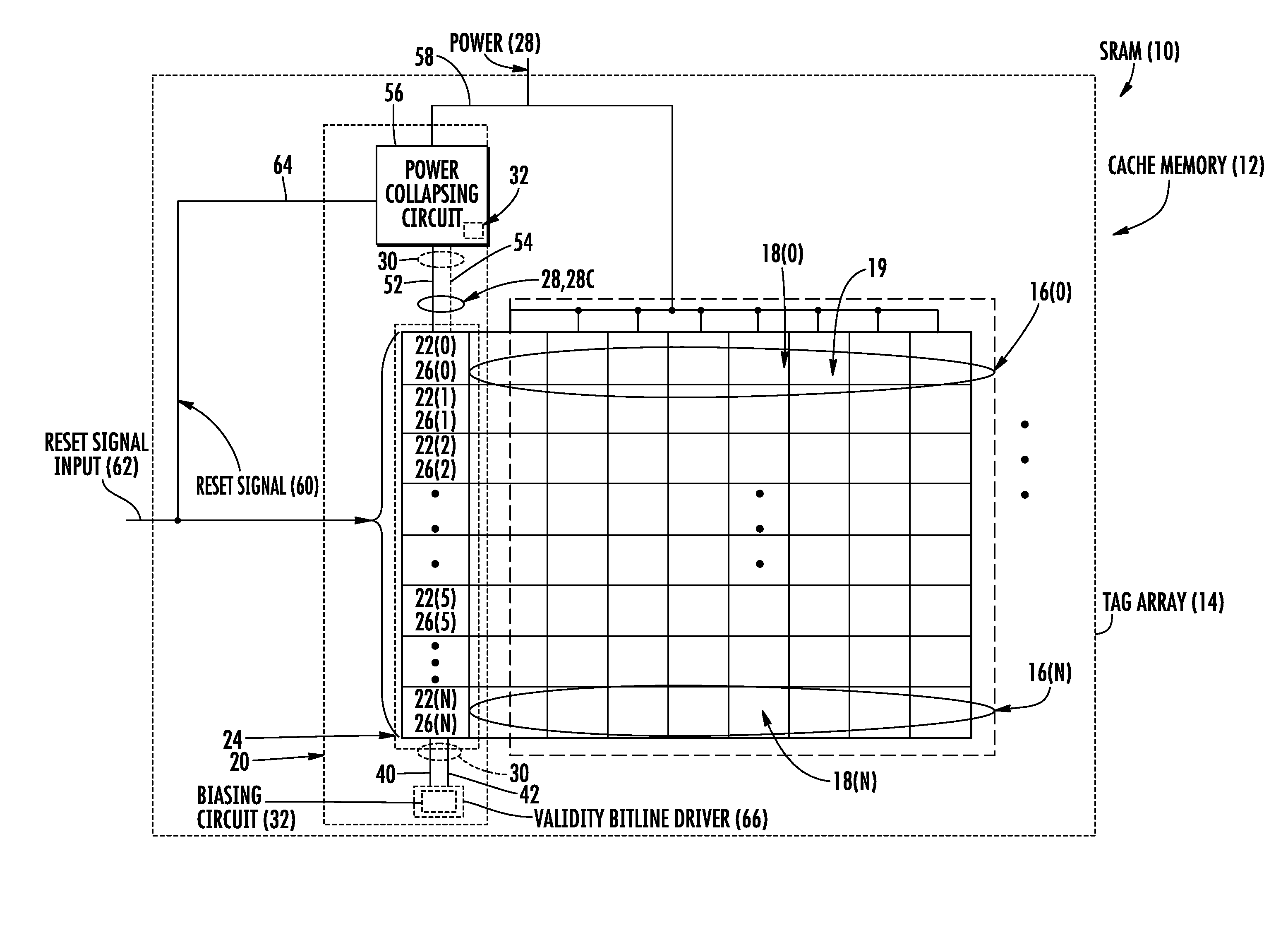
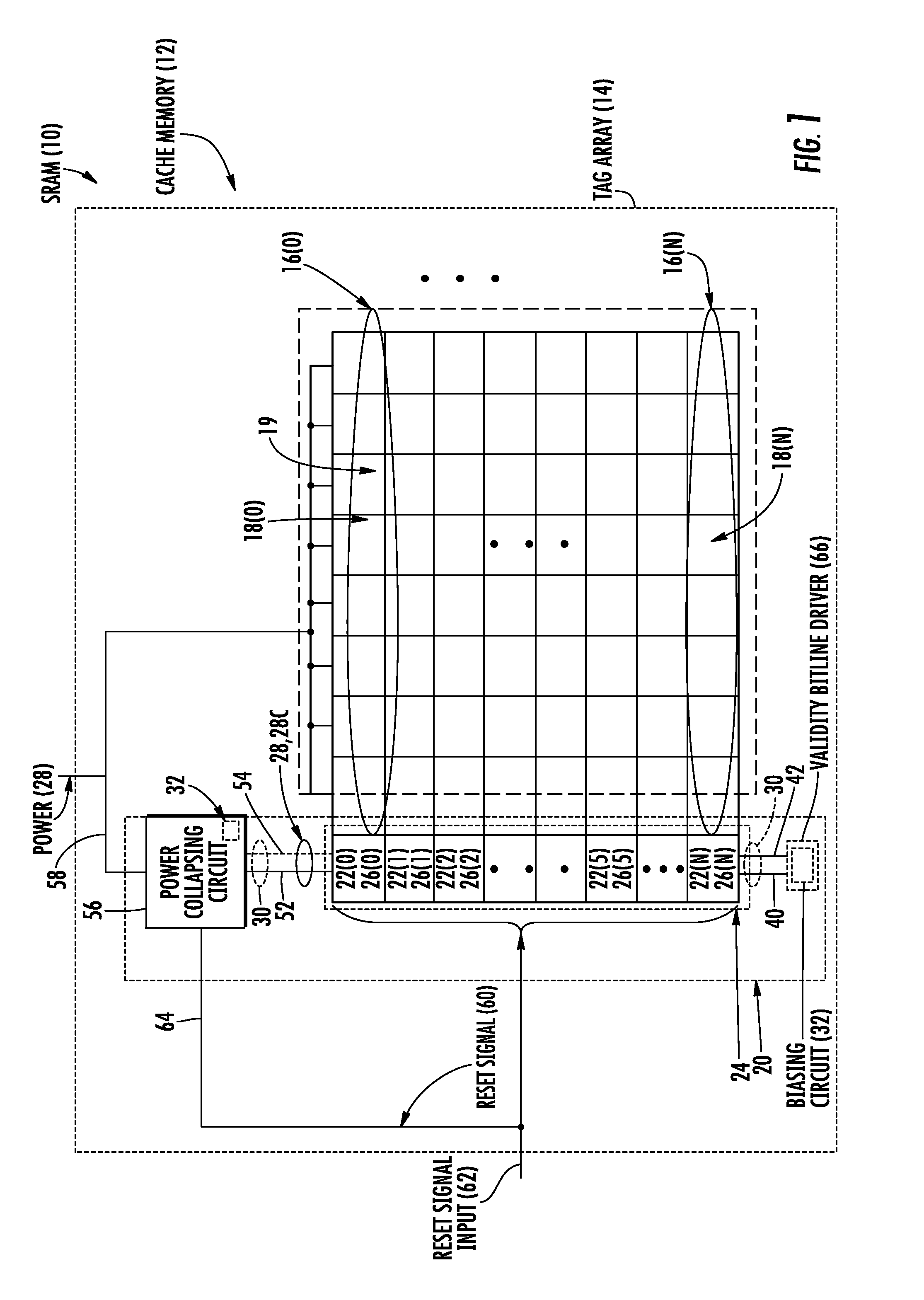
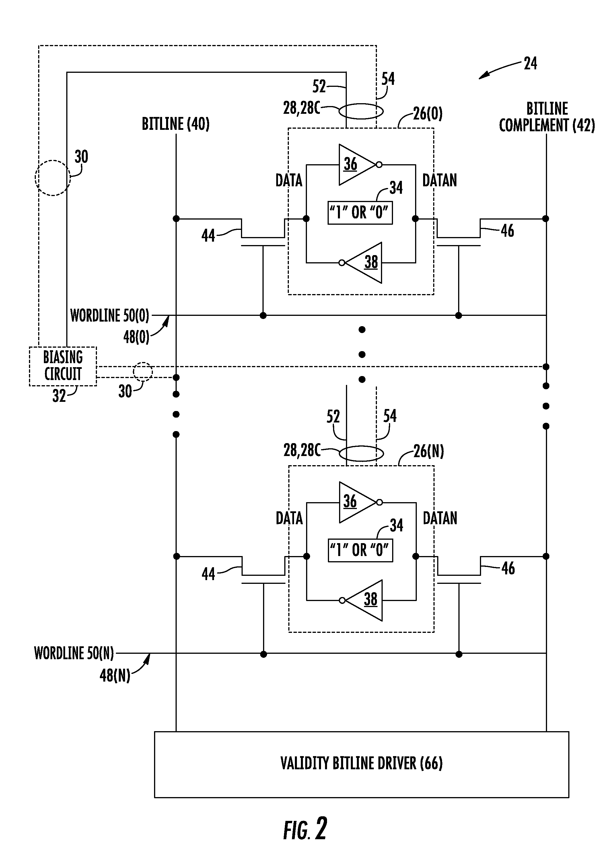
[0025]With reference now to the drawing figures, several exemplary embodiments of the present disclosure are described. The word “exemplary” is used herein to mean “serving as an example, instance, or illustration.” Any embodiment described herein as “exemplary” is not necessarily to be construed as preferred or advantageous over other embodiments.

[0026]Embodiments disclosed in the detailed description include circuits for voltage or current biasing static random access memory (SRAM) bitcells during SRAM reset operations. Related systems and methods are also disclosed. As one non-limiting example, the SRAM bitcells are included in an SRAM cache memory provided in a central processing unit (CPU) system. It may be desired to reset a plurality of SRAM bitcells to a desired state in a single reset operation, as opposed to a more time consuming method of resetting the state of each SRAM bitcell individually. For example, it may be desired to perform a reset invalidate operation for inval...


PUM


Abstract

Circuits for voltage or current biasing static random access memory (SRAM) bitcells during SRAM reset operations are disclosed. Related systems and methods are also disclosed. To reset a plurality of SRAM bitcells in a single reset operation, a biasing circuit is provided and coupled to the plurality of SRAM bitcells. The biasing circuit is configured to apply a voltage or current bias to the SRAM bitcells during a reset operation after power provided to the SRAM bitcells is collapsed to a collapsed power level below an operational power level. The bias is applied as the power to the SRAM bitcells is restored to an operational power level, thus forcing the SRAM bitcells into a desired state. In this manner, the SRAM bitcells can be reset in a single reset operation without need for an increased drive strength from a reset circuit and without need to provide specialized SRAM bitcells.

Description

PRIORITY CLAIM[0001]The present application claims priority to U.S. Provisional Patent Application Ser. No. 61 / 859,998 filed on Jul. 30, 2013 and entitled “CIRCUITS FOR BIASING STATIC RANDOM ACCESS MEMORY (SRAM) BITCELLS DURING SRAM RESET OPERATIONS, AND RELATED SYSTEMS AND METHODS,” which is incorporated herein by reference in its entirety.BACKGROUND[0002]I. Field of the Disclosure[0003]The technology of the disclosure relates to static random access memory (SRAM) bitcells and resetting of SRAM bitcells.[0004]II. Background[0005]A memory cell is a basic building block of computer data storage, also known as “memory.” A computer system may either read data from or write data to memory. There are different types of memory. For example, one type of memory is static random access memory (SRAM). As an example, SRAM may be used as cache memory in a central processing unit (CPU) system. A SRAM cache memory may be comprised of a tag array and a data array. The tag array receives a memory a...

Claims


Application Information

Patent Timeline
Patent Type & Authority Applications(United States)
IPC IPC(8): G11C11/412
CPCG11C11/412G11C7/20G11C11/417G11C11/419
Inventor CHAI, CHIAMINGMAURYA, SATENDRA KUMAR
Owner QUALCOMM INC
Why Eureka
Try Eureka