Semiconductor device

a technology of semiconductor devices and devices, applied in the direction of individual semiconductor device testing, semiconductor/solid-state device details, instruments, etc., can solve the problems of user wiring work that should be done by the user, miswiring may occur, etc., and achieve the effect of improving user convenience in wiring work

Active Publication Date: 2015-02-12
MITSUBISHI ELECTRIC CORP
View PDF8 Cites 17 Cited by
  • Summary
  • Abstract
  • Description
  • Claims
  • Application Information

AI Technical Summary

Benefits of technology

[0010]The present invention has been implemented to solve the above-described problems and it is an object of the present invention to improve user convenience in wiring work using a semiconductor device that allows a user to choose a current detection scheme.

Problems solved by technology

Moreover, when the above-described alternative of the current detection scheme is given, the burden of wiring work that should be done by the user increases.
As a result, miswiring may occur.

Method used


Image

  • Semiconductor device
  • Semiconductor device
  • Semiconductor device

Examples


first embodiment

Circuit of First Embodiment

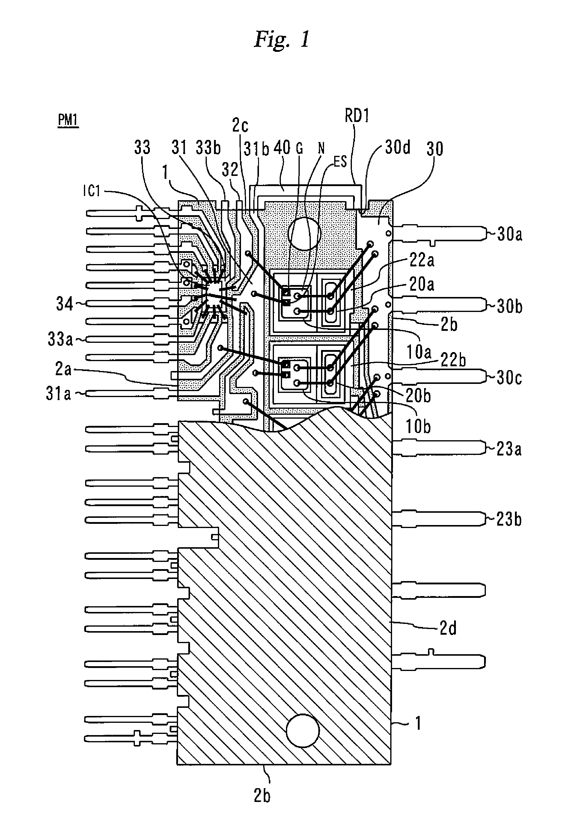
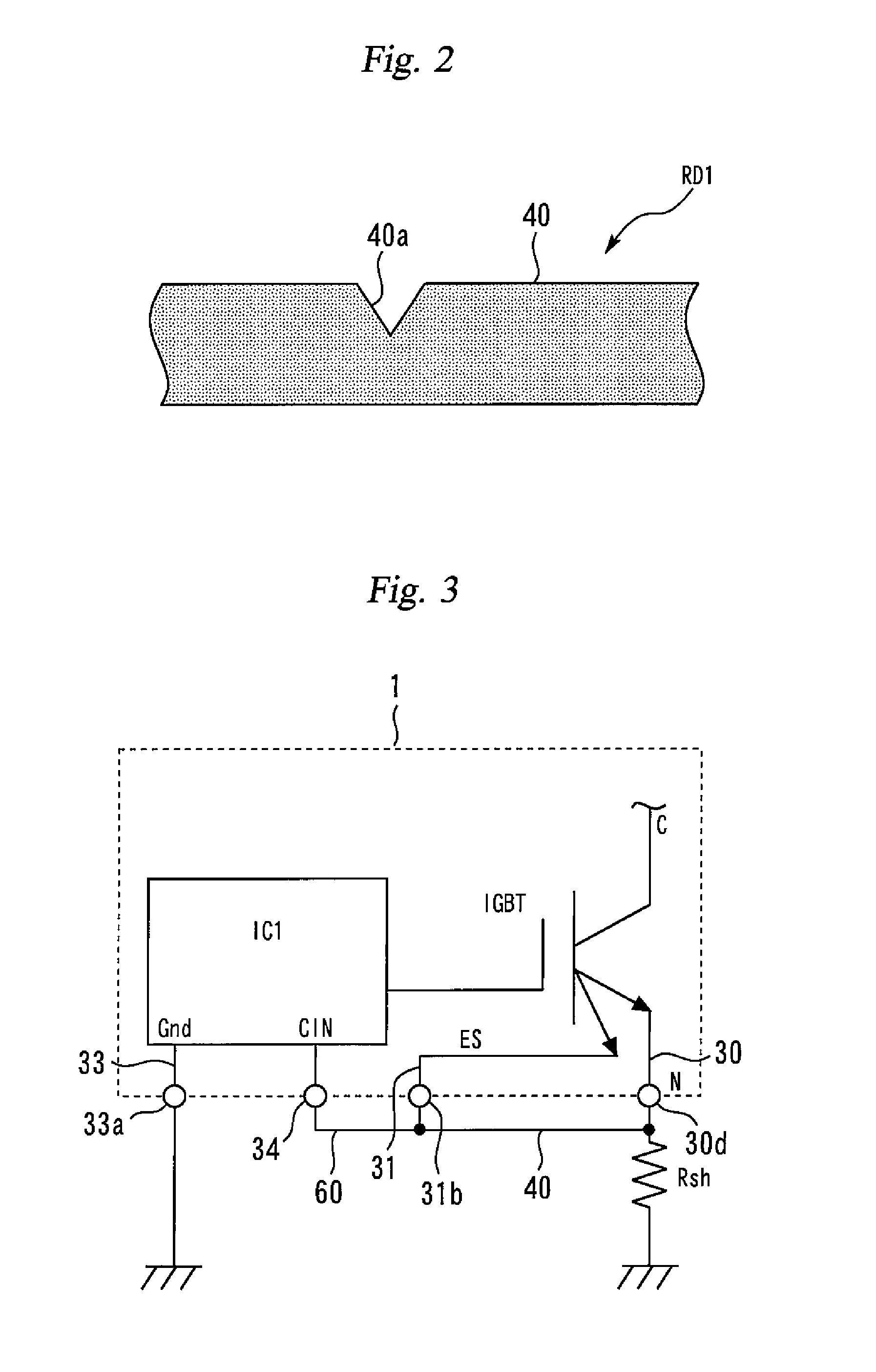
[0046]FIG. 3 and FIG. 4 illustrate the semiconductor device PM1 according to the first embodiment of the present invention and illustrate part of the inner circuit of the semiconductor device PM1. Parts assigned the same reference numerals between the structural diagram shown in FIG. 1 and the circuit diagrams shown in FIG. 3 and FIG. 4 are associated with each other in a one-to-one correspondence.

(Main Current Detection Scheme)

[0047]FIG. 3 illustrates a circuit in the case of adopting a current detection scheme for detecting a main current when the semiconductor device PM1 is mounted. In this case, an external shunt resistor Rsh is provided for a mounting substrate (not shown) on which the semiconductor device PM1 is to be mounted. A wire 60 is formed for electrically connecting the end 31a and an end of the lead 34 on the mounting substrate side so as to connect the detection terminal CIN and the emitter sense electrode ES.

[0048]Here, when the scheme of ...

second embodiment

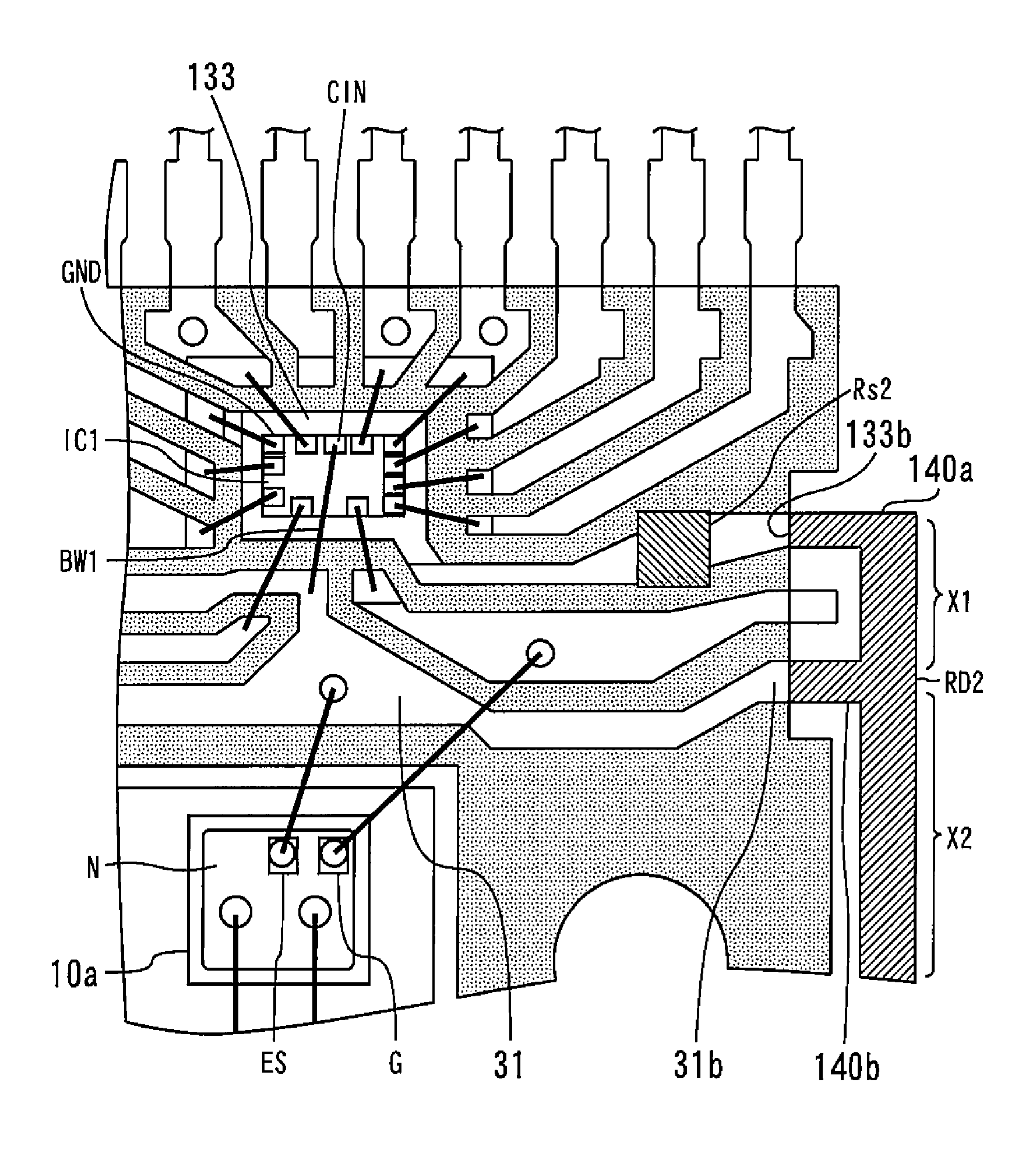
[0060]FIG. 6 and FIG. 7 illustrate a semiconductor device PM2 according to a second embodiment of the present invention. FIG. 6 has a format similar to that in FIG. 1 of the first embodiment, and is a plan view of the semiconductor device PM2, showing a perspective view of part of an inner structure thereof. FIG. 7 is an enlarged view of the periphery of the semiconductor element 10a and the integrated circuit IC1 in FIG. 6.

[0061]The semiconductor device PM2 has a configuration similar to that of the semiconductor device PM1 according to the first embodiment except in that a lead RD2 is provided instead of the lead RD1 and the lead 33, and the integrated circuit IC1 has a different bonding wire connection. Therefore, components identical or corresponding to those in the first embodiment will be described, assigned the same reference numerals and description will be focused on differences from the first embodiment and description of common items will be simplified or omitted.

[0062]Th...


PUM


Abstract

A semiconductor device capable of simplifying wiring work is provided. A semiconductor device includes a semiconductor element (insulated gate bipolar transistor IGBT) provided with an emitter main electrode and an emitter sense electrode, an integrated circuit having a detection terminal and a mold resin body that seals the semiconductor element and the integrated circuit, and a lead. The lead is provided with an inner lead part sealed in the mold resin body and electrically connected to the emitter sense electrode, an inner lead part sealed in the mold resin body and electrically connected to the emitter main electrode, and an outer lead part connected to the lead part on one side, connected to the inner lead part on the other side and exposed outside the mold resin body.

Description

BACKGROUND OF THE INVENTION[0001]1. Field of the Invention[0002]The present invention relates to a semiconductor device.[0003]2. Background Art[0004]Conventionally, as is disclosed in Japanese Patent Laid-Open No. 9-139461, a semiconductor device is known, which has an appearance with a plurality of leads extending in parallel on one side of a mold resin body. This type of appearance is adopted among common integrated circuits. Manufacturing steps thereof generally include die bonding and wire bonding of a semiconductor chip on a lead frame, sealing of the lead frame with mold resin and then lead cutting whereby the lead frame is cut.[0005]Semiconductor elements provided with a current sense function are well known and power semiconductor modules incorporating such semiconductor elements are becoming widespread. There is also a scheme that detects a current by detecting a main current instead of using a current sense function. A technique is also known which provides these two curre...

Claims


Application Information

Patent Timeline
Patent Type & Authority Applications(United States)
IPC IPC(8): G01R31/04G01R19/00
CPCG01R19/0092G01R31/041H01L2224/48137H01L2224/48139H01L2224/48247H01L2224/49111H01L23/495H01L23/49562H01L23/49575H01L2924/13055H01L2224/0603H01L2224/48096H01L2924/00H01L2924/00012G01R1/0491G01R31/2623G01R31/261G01R31/265G01R21/06G01R31/67
Inventor NAKAMURA, HIROYUKI
Owner MITSUBISHI ELECTRIC CORP
Why Eureka
Try Eureka