
Whole-Chip Esd Protection Circuit and Esd Protection Method

Inactive Publication Date: 2015-02-26
MONTAGE TECHNOLOGY CO LTD
View PDF4 Cites 5 Cited by
  • Summary
  • Abstract
  • Description
  • Claims
  • Application Information

AI Technical Summary

Benefits of technology

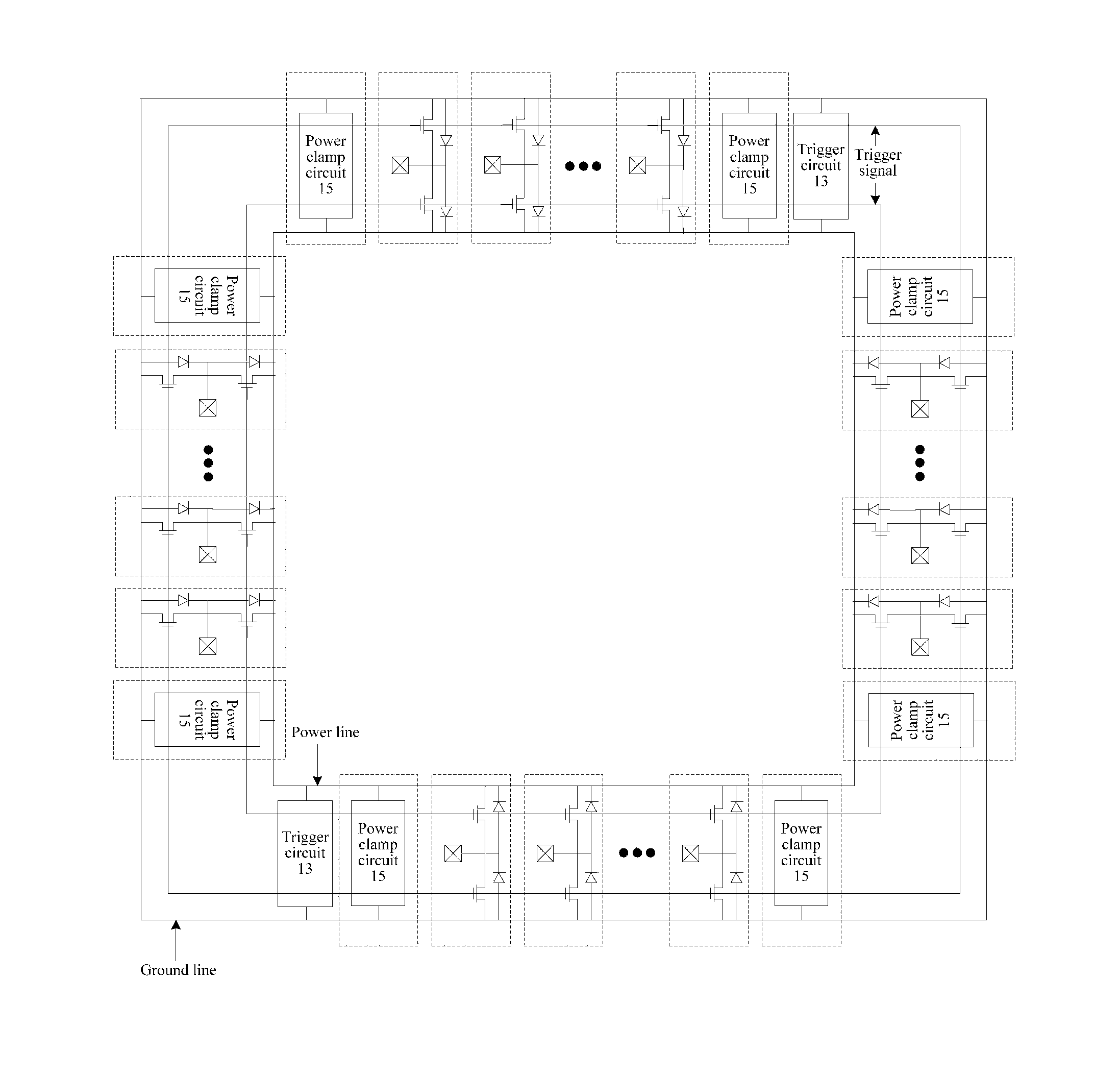
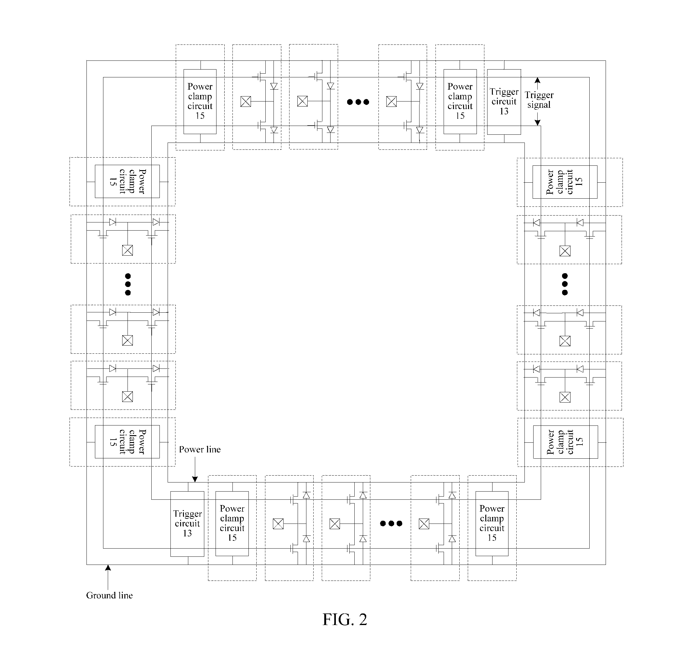
The present invention provides a whole-chip ESD protection circuit and method using existing driving transistors in the I / O units. Compared to previous configurations that require power clamps for each I / O unit, the present invention avoids the need for too many power clamps, reducing the size and cost of the chip. The whole-chip ESD protection circuit provides efficient and effective protection against ESD with multiple discharge paths. Overall, the present invention solves the problem of size and cost increase caused by power clamps and provides a more efficient and effective whole-chip ESD protection solution.

Problems solved by technology

ESD (Electrostatic Discharge) has become one of the most critical reliability issues in integrated circuits, which leads to failure or damage to power electronic device and the integrated circuit (IC) function thereof because static electricity is often generated during manufacturing, packaging, testing, and use procedures of devices.
For example, ESD events may be caused by accidental contact between two electrically charged objects and the following buildup of discharge path, thus resulting in device failure or even permanent damage.
Therefore, the ESD protection issue has always been one of the important issues in IC design field.
However, the continuous increasing IC scale and the introduction of new device concepts have brought in many new ESD challenges.
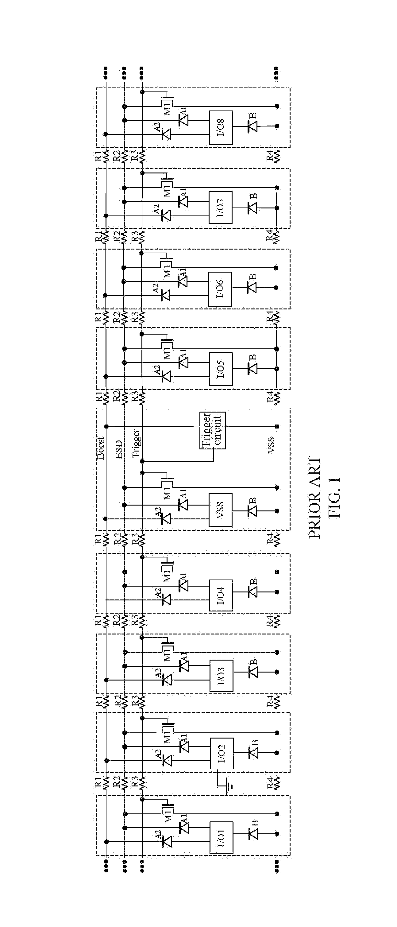
According to the prior art shown in FIG. 1, each I / O unit requires to be configured with a power clamp circuit, and consequently, the overall size and the cost of the chip are unnecessarily and significantly increased.

Method used


Image

  • Whole-Chip Esd Protection Circuit and Esd Protection Method
  • Whole-Chip Esd Protection Circuit and Esd Protection Method
  • Whole-Chip Esd Protection Circuit and Esd Protection Method

Examples


Embodiment Construction

[0031]In the prior art, distributed power clamp circuits are used in the chip, and each I / O unit requires to be configured with a power clamp circuit; consequently, the overall size and the cost of the chip are significantly increased. Therefore, the inventor of the present invention has made improvement and proposes a whole-chip ESD protection circuit and protection method. The whole-chip ESD protection circuit includes: an ESD trigger circuit located between a power line and a grounding wire and connected to multiple I / O units, and a power clamp circuit located between the power line and the grounding wire and connected to the ESD trigger circuit. The whole-chip ESD protection method includes: providing an ESD protection device which includes an ESD trigger circuit and a power clamp circuit that are located between a power line and a grounding wire, and are connected to multiple I / O units, to prevent the I / O units from an ESD damage; and the ESD trigger circuit generating an ESD t...


PUM


Abstract

A whole-chip Electrostatic Discharge (ESD) protection circuit and protection method are provided. The whole-chip ESD protection circuit comprises: input / output (I / O) units located between a power line and a grounding wire; a power clamp circuit located between the power line and the grounding wire and connected to the I / O units, any power clamp circuit being shared by multiple I / O units; and an ESD trigger circuit located between the power line and the grounding wire. The ESD trigger circuit generates an ESD trigger signal when an ESD events occurs and transmits the ESD trigger signal to the power clamp circuit and each I / O unit so that the power clamp circuit and each I / O unit form a current discharge path from the power line to the grounding wire respectively. Compared with the prior art, the present invention fully utilizes an existing driving transistor in the I / O unit to realize efficient whole-chip ESD protection and avoids adding too many power clamp circuits in the whole chip with regard to ESD, thereby reducing the overall size of the chip and lowering the cost.

Description

CROSS REFERENCE TO RELATED PATENT APPLICATION[0001]The present application claims the priority of the Chinese patent application No. 201310376740.0 filed on Aug. 26, 2013, which application is incorporated herein by reference.BACKGROUND OF THE PRESENT INVENTION[0002]1. Field of Invention The present invention relates to an Electrostatic Discharge (ESD) protection technology, and particularly to a whole-chip ESD protection circuit and ESD protection method.[0003]2. Description of Related Arts[0004]With rapid development of intelligent power process and high-power semiconductor devices, electronic products is becoming increasingly miniaturized and portable, thus increasing the application of power electronic devices. ESD (Electrostatic Discharge) has become one of the most critical reliability issues in integrated circuits, which leads to failure or damage to power electronic device and the integrated circuit (IC) function thereof because static electricity is often generated during m...

Claims


Application Information

Patent Timeline
IPC IPC(8): H02H9/04
CPCH02H9/049H02H9/047H01L27/0292
Inventor CAO, XIANGNINGWANG, YONG
Owner MONTAGE TECHNOLOGY CO LTD
Learn More