Device and Method to Additively Fabricate Structures Containing Embedded Electronics or Sensors

a technology of embedded electronics or sensors, applied in the field of additive manufacturing methods and systems, can solve the problems of inability to manufacture custom or non-planar sensors inside the structure of the produced part, inability to manufacture traditional fabrication methods, and inability to manufacture traditional prototypes & manufacturing with traditional fabrication methods, etc., to achieve the effect of reducing the force required and high viscosity

Inactive Publication Date: 2015-03-19
NORTHEASTERN UNIV
View PDF0 Cites 73 Cited by
  • Summary
  • Abstract
  • Description
  • Claims
  • Application Information

AI Technical Summary

Benefits of technology

[0019]In one aspect, the invention includes a nozzle design that reduces the force required to expell high viscosity material from the ...

Problems solved by technology

An object with complex freeform three-dimensional (3D) contours can be very challenging and very costly to prototype & manufacture with traditional fabrication methods.
Current Additive Manufacturing processes do not support the direct fabrication of objects that contain embedded electronics or sensors.
For standard components this is labor-intensive but functional, however for fabricating custom or non-planar sensors inside the structure of the produced part this not feasible.
As the conductive material is pushed along the pathways the reliability of complete filling is questionable from sharp bends and bifurcations in the channels.
This accomplishes the goal of embedding electronics in the components but with significant limitations and uncertainties.
This method of manufacturing has many limitations.
It can be difficult to force the silicone all the way through a complicated channel without breaking the path of the silicone at any point, or causing irregularities and uneven areas.
The likelihood of breaks in t...

Method used


Image

  • Device and Method to Additively Fabricate Structures Containing Embedded Electronics or Sensors
  • Device and Method to Additively Fabricate Structures Containing Embedded Electronics or Sensors
  • Device and Method to Additively Fabricate Structures Containing Embedded Electronics or Sensors

Examples


Embodiment Construction

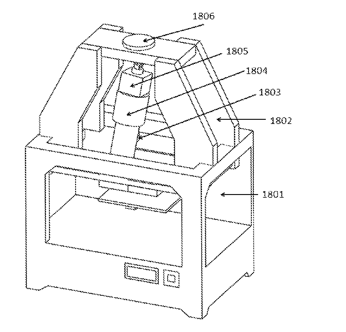
[0053]The Embedded Electronics by Layered Assembly (EELA) system is a motorized extruder that can be used to extrude a piezoresistive elastomer, such as a conductive silicone compound, into channels built during the additive manufacturing process on a 3D printer. The EELA system enables the building of conductive circuitry directly into an object while the object is being printed, rather than requiring the injection of the conductive material after the 3D printing is completed. The EELA system is capable of more fine-tuned and precise movements than a person can make with a syringe, and since printing and extrusion occur together, the EELA system may easily reach all areas of the conductive path in the object since it has access to the cross section of each layer during the build. This eliminates the potential problems described above and requires less overall work during manufacturing. Additionally, this can help to standardize the process of embedding conductive materials.

[0054]FI...


PUM

PropertyMeasurementUnit
Temperatureaaaaaaaaaa
Pressureaaaaaaaaaa
Electrical conductivityaaaaaaaaaa

Abstract

A method of constructing an object includes depositing a first material in a predetermined arrangement to form a structure. The method further includes depositing a second material within the structure. The second material may have electrical properties and the method also includes providing electrical access to the second material to enable observation of the one or more electrical properties.

Description

CROSS REFERENCE TO RELATED APPLICATIONS[0001]This application claims benefit of the following Patent Applications, the contents of which are hereby incorporated by reference in their entirety: U.S. Provisional Patent Application Ser. No. 61 / 638,576, filed Apr. 26, 2012 and U.S. Provisional Patent Application Ser. No. 61 / 804,440, filed Mar. 22, 2013.BACKGROUND[0002]1. Field of Invention[0003]This invention generally relates to methods and systems of Additive Manufacturing. More particularly, the invention relates to a motorized hardware extruder that can inject or extrude a conductive material (for example, a piezoresistive elastomer) into parts as they are being fabricated by a 3D printer or other Additive Manufacturing system.[0004]2. Description of Related Art[0005]An object with complex freeform three-dimensional (3D) contours can be very challenging and very costly to prototype & manufacture with traditional fabrication methods. Additive Manufacturing (AM), also known as “3D Pri...

Claims


Application Information

Patent Timeline
IPC IPC(8): B29C67/00H01C10/10
CPCB29C67/0055B29C67/0088H01C10/10B29K2083/00B29K2507/04B29L2031/34B29K2505/08B29K2995/0005B33Y10/00B33Y80/00B33Y30/00B33Y50/00B33Y40/00B29K2995/0003B29C70/88H05K3/0014H05K3/0091H05K2201/0218H05K2201/0314H05K2201/0323H05K2201/0376H05K2203/0759H05K1/16H05K3/1258H05K2201/10151B29C64/118B29C64/106
Inventor RANKY, RICHARDCARVER, ALEXANDRAMAVROIDIS, CONSTANTINOSLANDERS, DANIELSIVAK, MARK L.
Owner NORTHEASTERN UNIV
Why Eureka
Try Eureka