Group III Nitride Heterostructure for Optoelectronic Device

Active Publication Date: 2015-03-26
SENSOR ELECTRONICS TECH
View PDF0 Cites 48 Cited by
  • Summary
  • Abstract
  • Description
  • Claims
  • Application Information

AI Technical Summary

Benefits of technology

[0015]Aspects of the invention provide heterostructures for use in optoelectronic devices and the resulting optoelectronic devices. One or more parameters of the heterostructure can be configured to improve the reliability of the corresponding optoelectronic device. The materials used to create the active structure of the device can be considered in configuring various parameters the n-type and/or p-type sides of the heterostructure.
[0016]A first aspect of the invention provides a heterostructure comprising: a substrate; an AlN buffer layer located on the substrate; a AlxGa1-xN/Alx′Ga1-x′N first superlattice structure located on the buffer layer, wherein 0.6<x≦1, 0.1<x′<0.9, and x>x′, and wherein each layer in the first superlattice structure has a thickness less than or equal to one hundred nanometers; a AlyGa1-yN/Aly′Ga1-y′N second superlattice structure located on the first superlattice structure, wherein y′<x′, 0.6<y≦1, 0.1<y′<0.8, and y>y′, and wherein each layer in the second superlattice structure has a thickness less than one hundred nanometers; an AlzGa1-zN n-type layer located on the second superlattice structure, wherein 0.1<z<0.85 and z<y′; and an AlbGa1-bN/AlqGa1-qN active structure, wherein b-q>0.05.
[0017]A second aspect of the invention provides a heterostructure comprising: a substrate; a buffer layer located on the substrate, wherein the buffer layer is formed of a group III nitride material including aluminum; a grading structure located on the buffer layer, wherein the grading structure is formed of a group III nitride material having an aluminum molar fraction that decreases from an aluminum molar fraction at a bottom heterointerface to an aluminum molar fraction at a top heterointerface; a n-type layer located on the grading structure, wherein the n-type layer is formed of a group III nitride material including aluminum having a molar fraction z, and wherein 0.1<z<0.85; an active structure including quantum wells and barriers, wherein the quantum wells are formed of a group III nitride material including aluminum having a molar fraction q and the barriers are formed of a grou

Problems solved by technology

When the stresses become larger than threshold stresses, the reliability of a structure can be compromised due to the formation of carrier capturing defects during the operation of the device.
The conducting characteristics of the device also can be altered during device operation due to formation of cracks and defects.
Furthermore, a resultant junction temperature increase can further affect the reliability and efficie

Method used


Image

  • Group III Nitride Heterostructure for Optoelectronic Device
  • Group III Nitride Heterostructure for Optoelectronic Device
  • Group III Nitride Heterostructure for Optoelectronic Device

Examples


Embodiment Construction

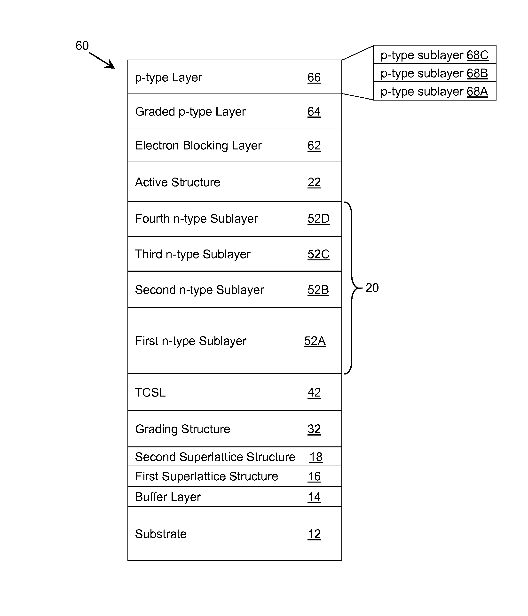
[0033]As indicated above, aspects of the invention provide heterostructures for use in optoelectronic devices and the resulting optoelectronic devices. One or more parameters of the heterostructure can be configured to improve the reliability of the corresponding optoelectronic device. The materials used to create the active structure of the device can be considered in configuring various parameters the n-type and / or p-type sides of the heterostructure.

[0034]An illustrative embodiment can improve the reliability of a device through simultaneous optimization of several parameters of the heterostructure. These parameters can include: compositional profiles of the semiconductor layers; doping profiles of the semiconductor layers; and thicknesses of the semiconductor layers. Additionally, optimization of strains within the semiconductor layers and resultant polarization fields also can increase a reliability of the corresponding device.

[0035]As used herein, unless otherwise noted, the t...


PUM


Abstract

Heterostructures for use in optoelectronic devices are described. One or more parameters of the heterostructure can be configured to improve the reliability of the corresponding optoelectronic device. The materials used to create the active structure of the device can be considered in configuring various parameters the n-type and/or p-type sides of the heterostructure.

Description

REFERENCE TO RELATED APPLICATIONS[0001]The current application claims the benefit of co-pending U.S. Provisional Application No. 61 / 881,192, titled “Group III Nitride Heterostructure for Ligth Emission and Sensing,” which was filed on 23 Sep. 2013, and which is hereby incorporated by reference.TECHNICAL FIELD[0002]The disclosure relates generally to optoelectronic devices, and more particularly, to group III nitride heterostructures for use in fabricating optoelectronic devices.BACKGROUND ART[0003]Development of electronic and optoelectronic devices, such as group III nitride based light emitting diodes (LEDs), with high efficiency and reliability depends on many factors. Such factors include: the quality of the semiconductor layers, active layer design, and contact quality. Designing high quality semiconductor layers is especially important for a number of electronic and optoelectronic devices including ultraviolet light emitting diodes (UV LEDs). The quality of a semiconductor lay...

Claims


Application Information

Patent Timeline
IPC IPC(8): H01L33/00H01L33/12H01L33/14H01L33/06
CPCH01L33/0025H01L33/06H01L33/145H01L33/12H01L33/0075H01L33/007H01L33/04H01L33/32
Inventor JAIN, RAKESHSHATALOV, MAXIM S.YANG, JINWEIDOBRINSKY, ALEXANDERSHUR, MICHAELGASKA, REMIGIJUS
Owner SENSOR ELECTRONICS TECH
Why Eureka
Try Eureka