Substrate processing device and substrate processing method

Inactive Publication Date: 2015-04-02
SHIBAURA MECHATRONICS CORP
View PDF3 Cites 5 Cited by
  • Summary
  • Abstract
  • Description
  • Claims
  • Application Information

AI Technical Summary

Benefits of technology

The invention is a device and method that can replace the cleaner on a substrate surface with a solvent that evaporates quickly. This prevents the pattern on the substrate from collapsing during the drying process.

Problems solved by technology

In the drying, there are problems that occur with patterns, e.g., around memory cells and gates collapses due to miniaturization according to increase in integration degree and capacity of the semiconductors in recent years.

Method used


Image

  • Substrate processing device and substrate processing method
  • Substrate processing device and substrate processing method
  • Substrate processing device and substrate processing method

Examples


Embodiment Construction

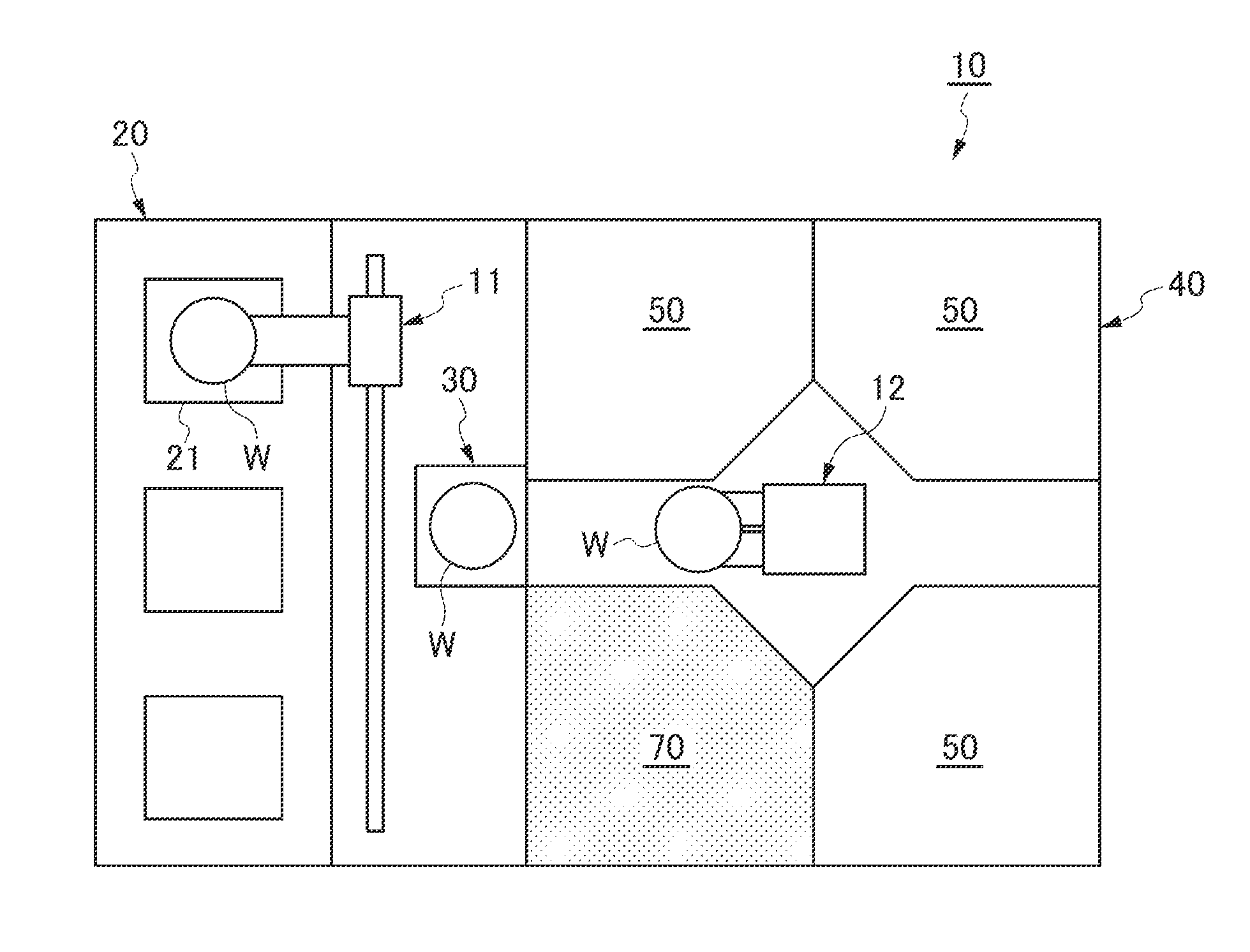
[0028]A substrate processing device 10 includes, as illustrated in FIG. 1, a substrate supply / discharge unit 20, a substrate storing buffer unit 30, and a plurality of substrate processing chambers 40. A transporting robot 11 is arranged between the substrate supply / discharge unit 20 and the substrate storing buffer unit 30, and a transporting robot 12 is arranged between the substrate storing buffer unit 30 and the substrate processing chamber 40. The substrate processing chamber 40 is formed of a set of a substrate cleaning chamber(s) 50 and a substrate drying chamber(s) 70, as will be described later.

[0029]The substrate supply / discharge unit 20 can transfer a plurality of substrate storing cassettes 21 therefor and thereto. The substrate storing cassette 21 stores a plurality of substrates W such as unprocessed wafers, liquid crystal substrates and the like, and is transferred into the substrate supply / discharge unit 20. The substrate storing cassette 21 stores the substrates W p...


PUM


Abstract

In a substrate processing device 10, a magnetic field forming unit is added to a solvent supply unit 58. The magnetic field forming unit 100 applies a magnetic field to a surface of a substrate W on which a cleaning liquid and a volatile solvent coexist. The magnetic field forming unit stirs and mixes the cleaning liquid and the volatile solvent on the surface of the substrate W to promote replacement of the cleaning liquid with the volatile solvent.

Description

[0001]The disclosure of Japanese Patent Application No. 2013-215126 filed Sep. 30, 2013 and Japanese Patent Application No. 2014-139197 filed Jul. 4, 2014 including specifications, drawings and claims is incorporated herein by reference in its entirety.FIELD OF THE INVENTION[0002]The present intention relates to a substrate processing device and a substrate processing method.[0003][Related Art][0004]In manufacturing semiconductors and others, a substrate processing device supplies a processing liquid to a surface of a substrate of a wafer, a liquid crystal substrate or the like to process a surface of the substrate, then supplies a cleaning liquid such as ultrapure water to the substrate surface to clean the substrate surface, and further dries it.[0005]In the drying, there are problems that occur with patterns, e.g., around memory cells and gates collapses due to miniaturization according to increase in integration degree and capacity of the semiconductors in recent years. This is ...

Claims


Application Information

Patent Timeline
IPC IPC(8): B08B7/04B08B3/08B08B7/00B08B3/02
CPCB08B7/04B08B7/0071B08B3/08B08B3/022H01L21/67028H01L21/67051
Inventor NAGASHIMA, YUJIMATSUSHITA, JUNSAITO, YUKIHAYASHI, KONOSUKEMIYAZAKI, KUNIHIRO
Owner SHIBAURA MECHATRONICS CORP
Why Eureka
Try Eureka