Light emitting device

a technology of light emitting device and light source, which is applied in the direction of solid-state devices, semiconductor devices, lighting and heating apparatus, etc., can solve the problems that the need for initial brightness cannot be satisfied insufficiently, and achieve the effect of simple configuration and efficient extraction

Active Publication Date: 2015-04-02
NICHIA CORP
View PDF5 Cites 5 Cited by
  • Summary
  • Abstract
  • Description
  • Claims
  • Application Information

AI Technical Summary

Benefits of technology

[0010]According to this disclosure, it is possible to provide the light emitting device of the disclosure which light can be extracted more efficiently with simple configuration.

Problems solved by technology

Even when a light scattering layer is provided, depending on the type of metal member disposed on the substrate surface where the light emitting element is installed, the light emitted from the light emitting element can be absorbed, so at present the need for initial brightness in particular cannot be sufficiently satisfied.

Method used


Image

  • Light emitting device
  • Light emitting device
  • Light emitting device

Examples


embodiment 1

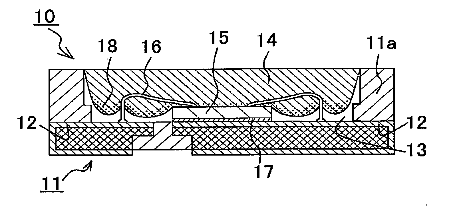
[0087]As shown in FIGS. 1A and 1B, the light emitting device 10 in this embodiment comprises a substrate 11 having metal 12 on its surface, light emitting elements 15 installed on the surface of the substrate 11, wires 16 that are electrically connected to the light emitting elements 15 and the metal 12, and a light reflecting member 13 that covers the metal 12. It also comprises a translucent member 14 that covers the light emitting elements 15 and the light reflecting member 13.

[0088]The substrate 11 has the metal 12, which is formed as a wiring pattern by the vapor deposition of Ti, Pd, and Au on the surface of a flat material composed of an aluminum nitride ceramic, and Au plating is applied over this metal 12. The substrate 11 also has a wall 11a that surrounds the light emitting elements 15. The wall 11a has a step at about the same height as the surface of the light emitting elements 15, and the total height is about three times the thickness of the light emitting element.

[00...

embodiment 2

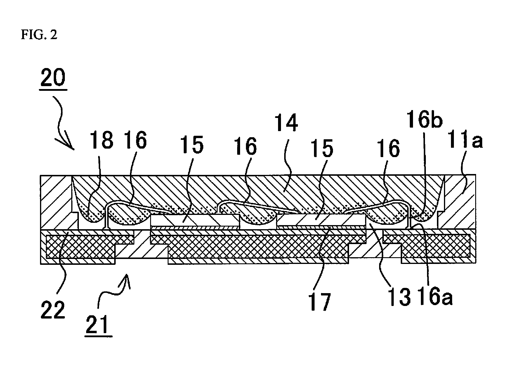
[0106]As shown in FIG. 2, the light emitting device 20 in this embodiment is configured substantially the same as the light emitting device 10 in Embodiment 1, except that there are two light emitting elements 15 connected in series, and a corresponding substrate 21 and metal 22 pattern is used. In this case, a ball stitch on ball is formed on the electrode of one of the light emitting elements 15 in order to connect the light emitting elements 15 together.

[0107]The light emitting device in this embodiment has the same effect as that in Embodiment 1.


PUM

PropertyMeasurementUnit
thicknessaaaaaaaaaa
thicknessaaaaaaaaaa
diameteraaaaaaaaaa

Abstract

A light emitting device of the invention includes a substrate having a metal on a surface thereof; a light emitting element installed on the surface of the substrate; a wire that connects the light emitting element and the metal; and a light reflecting member that covers the metal, the wire having a first bonding ball that is disposed on a surface of the metal, and an extension that extends above the first bonding ball, and the light reflecting member having a protrusion over the first bonding ball.

Description

CROSS-REFERENCE TO RELATED APPLICATION[0001]This application claims priority to Japanese Patent Application No. 2013-203704, filed on Sep. 30, 2013. The entire disclosure of Japanese Patent Application No. 2013-203704 is hereby incorporated herein by reference.BACKGROUND OF THE INVENTION[0002]1. Field of the Invention[0003]The present invention relates to a light emitting device, and more particularly relates to a light emitting device in which a light reflecting member is disposed around a light emitting element.[0004]2. Description of the Related Art[0005]A light emitting device has been proposed in the past in which a light scattering layer is disposed around a light emitting element that is compact and has good power efficiency, in order to efficiently utilize the light emitted from the end face of the light emitting element and thereby improve emission efficiency (JPH11-284234A, and JP2010-232203A).SUMMARY OF THE INVENTION[0006]Even when a light scattering layer is provided, de...

Claims


Application Information

Patent Timeline
Patent Type & Authority Applications(United States)
IPC IPC(8): F21V13/02F21V7/22
CPCF21V7/22F21V13/02H01L25/0753H01L33/508H01L33/62H01L2224/48091H01L2224/48137H01L2224/48465H01L2224/48471H01L2224/4945H01L2224/73265H01L2224/8592H01L2224/45144H01L2924/181H01L33/56H01L2924/00014H01L33/60H01L2924/00H01L2924/00012H01L2224/4554
Inventor OKURA, SHINYA
Owner NICHIA CORP
Why Eureka
Try Eureka