Light-emitting device and method for manufacturing light-emitting device

a technology of light-emitting devices and manufacturing methods, which is applied in the manufacture of semiconductor/solid-state devices, semiconductor devices, electrical devices, etc., can solve the problems of non-uniform brightness distribution of light-emitting surfaces, and achieve uniform brightness distribution, high luminous efficiency, and easy manufacturing

Inactive Publication Date: 2015-06-11
SHOWA DENKO KK
View PDF4 Cites 1 Cited by
  • Summary
  • Abstract
  • Description
  • Claims
  • Application Information

AI Technical Summary

Benefits of technology

[0021]According to the present invention, a light-emitting device using an electroluminescent element which has a high luminous efficiency, has a uniform brightness distribution in the light-emitting area and is easy to be manufactured is provided.

Problems solved by technology

Accordingly, when the light-emitting area is made large, a brightness distribution in the light-emitting surface becomes non-uniform.

Method used


Image

  • Light-emitting device and method for manufacturing light-emitting device
  • Light-emitting device and method for manufacturing light-emitting device
  • Light-emitting device and method for manufacturing light-emitting device

Examples


first exemplary embodiment

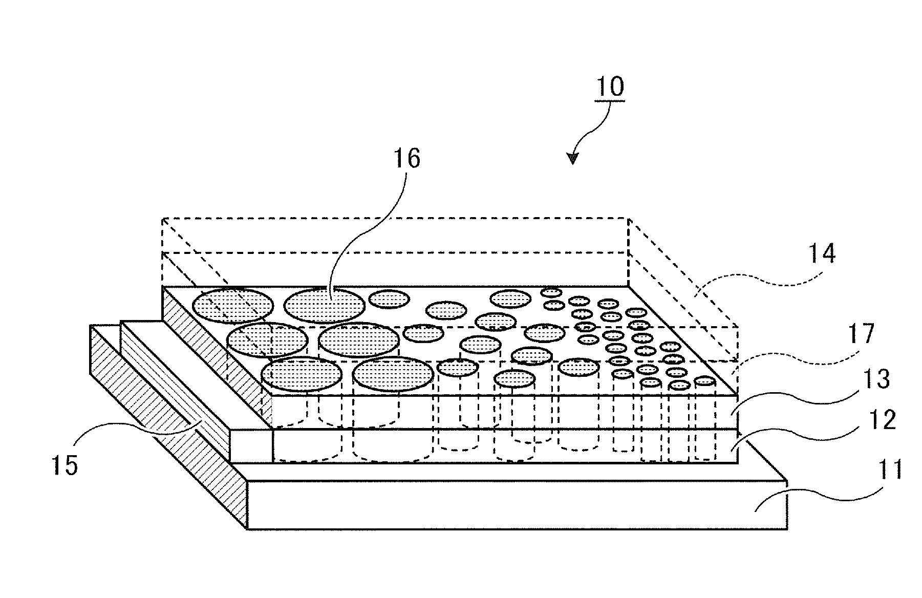
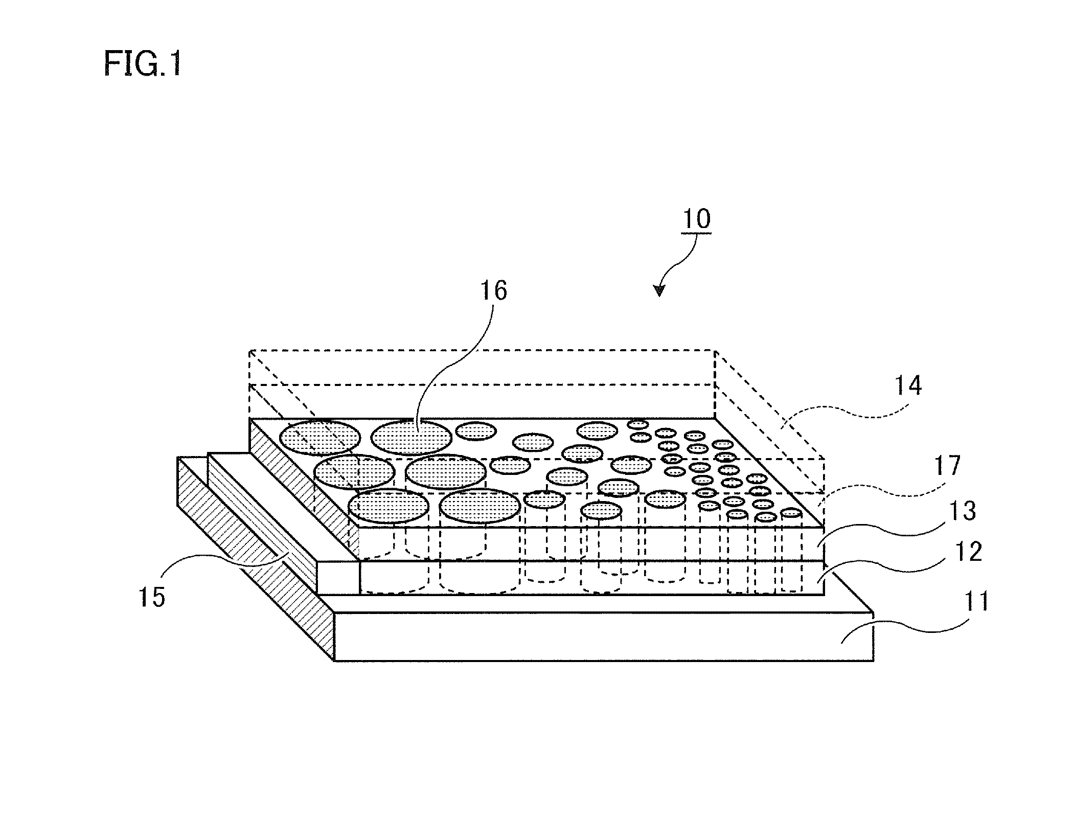
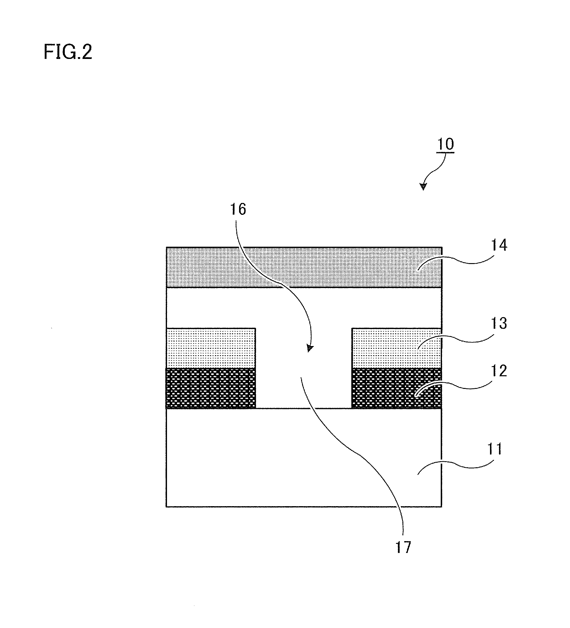
[0035]FIG. 1 is a diagram for illustrating the first exemplary embodiment of a light-emitting device 10 in the present exemplary embodiment. FIG. 2 is a partial cross-sectional view for illustrating a specific example of the light-emitting device 10 shown in FIG. 1. Hereinafter, the light-emitting device 10 will be explained with reference to FIGS. 1 and 2.

10>

[0036]In the light-emitting device 10, a substrate 11, an anode layer 12 as a first electrode layer for injecting holes, which is formed on the substrate 11 in the case where the substrate 11 side is assumed to be the downside, and a dielectric layer 13 that is formed on the anode layer 12 and has an insulating property are stacked in order. Moreover, a concave portion 16 that passes through the anode layer 12 and the dielectric layer 13 is formed. Further, a light-emitting portion 17 that is formed successively from an upper surface of the dielectric layer 13 to an inner surface of the concave portion 16 and includes a light-e...

second exemplary embodiment

[0145]FIG. 8 is a diagram for illustrating the second exemplary embodiment of a light-emitting device in the present exemplary embodiment.

[0146]In a light-emitting device 20 shown in FIG. 8, a substrate 21, an anode layer 22 as a first electrode layer for injecting holes, which is formed on the substrate 21 in the case where the substrate 21 side is assumed to be the downside, and a dielectric layer 23 that is formed on the anode layer 22 and has an insulating property are stacked in order, which is the same as in the light-emitting device 10 (refer to FIG. 1). Moreover, similarly to the light-emitting device 10, plural concave portions 26 that pass through the anode layer 22 and the dielectric layer 23 are formed, and a light-emitting portion 27 that is formed successively from an upper surface of the dielectric layer 23 to an inner surface of the concave portion 26 is formed. On an upper part of the light-emitting portion 27, a cathode layer 24 as a second electrode layer for inje...

example 1

Preparation of Light-Emitting Material Solution

Synthesizing of a Phosphorescent Light-Emitting Polymer Compound

[0151]A phosphorescent light-emitting polymer compound (A) was prepared in accordance with the method disclosed in the paragraph [0077] of International Publication No. WO2010-016512. The weight-average molecular weight of polymer compound (A) was 52000, and molar ratio of each repeating unit was k:m:n=6:42:52.

[0152]A light-emitting material solution (hereinafter, also referred to as “solution A”) was prepared by dissolving 3 parts by weight of the light-emitting polymer compound prepared (A) in 97 parts by weight of toluene.

Preparation of Organic Light-Emitting Element

[0153]A light-emitting device 1 having the similar cross-sectional shape as shown in FIG. 2 was produced in accordance with the order shown in FIG. 7.

[0154]A glass substrate (=the substrate 11: 110 mm square, 1 mm in thickness) in which ITO film (=the anode layer 12: 150 nm in thickness, sheet resistance 10Ω ...


PUM


Abstract

A light-emitting device (10) is provided with: a substrate (11); a light-emitting region including a light-emitting portion (17) formed to contact a first electrode layer (12) and a second electrode layer (14); and plural concave portions (16). The light-emitting portion contacting at least the first electrode layer and the dielectric layer in the concave portion. The light-emitting device further comprises a terminal (anode terminal) (15) formed outside the light-emitting region, and connecting one of the first electrode layer (12) and the second electrode layer (14) having larger sheet resistance to a power supply. In the light-emitting region, the plural concave portions (16) are formed such that the sum, per unit area, of a contour length of the planar shapes of the concave portions (16) on an upper face of the dielectric layer (13) increases from a region near the terminal (15) towards a region far from the terminal (15).

Description

TECHNICAL FIELD[0001]The present invention relates to a light-emitting device and a method of manufacturing a light-emitting device, in detail, relates to a light-emitting device and the like having high brightness uniformity and using an electroluminescent element with a configuration in which a light-emitting layer including a light-emitting material is sandwiched with a pair of electrodes.BACKGROUND ART[0002]An electroluminescent element has a configuration in which a light-emitting layer including a light-emitting material is sandwiched between an anode electrode and a cathode electrode, and is provided with a characteristics that a light-emission with high brightness is available with a low driving voltage. Therefore, the electroluminescent element is expected to be applied to an electro-optical device such as a display or an illumination.[0003]In recent years, for a purpose of improving a performance as an illumination usage, researches have been conducted on improving a light...

Claims


Application Information

Patent Timeline
Patent Type & Authority Applications(United States)
IPC IPC(8): H01L33/08H01L33/62H01L33/44H01L33/00H01L33/24
CPCH01L33/08H01L33/005H01L2933/0025H01L33/44H01L33/62H01L33/24H10K50/11H10K50/813H10K50/85
Inventor IMAI, NAOYUKITERASHIMA, TAKASHI
Owner SHOWA DENKO KK
Why Eureka
Try Eureka