Field-shaping multi-well avalanche detector for direct conversion amorphous selenium

a field-shaping, multi-well technology, applied in the direction of radiation intensity measurement, instruments, x/gamma/cosmic radiation measurement, etc., can solve the problems of low-dose imaging performance degradation, limited current direct conversion fpds, and use of photon-counting mode detection, etc., to achieve stable avalanche multiplication gain

Active Publication Date: 2015-06-18
THE RES FOUND OF STATE UNIV OF NEW YORK
View PDF2 Cites 13 Cited by
  • Summary
  • Abstract
  • Description
  • Claims
  • Application Information

AI Technical Summary

Benefits of technology

[0012]An aspect of the present invention provides a direct conversion amorphous selenium radiation detector structure that achieves stable avalanche multiplication gain and provides high-density insulated wells and field-shaping to eliminate formation of field hot-spots in an avalanche region and high fields at a metal-semiconductor interface to provide a semi-Gaussian field distribution inside each well using field-shaping electrodes and to provide an electric field at the metal-semiconductor interface of one order-of-magnitude lower than a peak value where avalanche occurs, thereby providing a practical direct conversion amorphous selenium detector with avalanche gain, and method for operation thereof.

Problems solved by technology

Disordered solids, which are easier and less expensive to develop than single crystalline solids, have not been utilized as photon-counting mode detection media because of low carrier mobility and transit-time-limited photo response.
However, current direct conversion FPDs are limited by, inter alia, degradation of low-dose imaging performance due to electronic noise, because energy required to generate an electron-hole pair in a-Se is 50 eV at 10 V / micron.
Although other photoconductive materials with higher conversion have been investigated, the other photoconductive materials suffer from charge trapping and manufacturing issues.
However, this electric field increase is extremely challenging for reliable detector construction and operation, and is virtually impractical.
Amorphous solids, i.e., non-crystalline solids with disorder, have been ruled out as viable radiation imaging detectors in a photon-counting mode because of low temporal resolution due to low carrier mobilities and transit-time limited pulse response, and low conversion gain of high energy radiation to electric charge.
However, significant obstacles prevent practical implementation of a direct conversion a-Se layer with separate absorption and avalanche regions.
However, a separate localized avalanche multiplication region has not been realized due to formation of field hot-spots, where F exceeds 150 V / μm, leading to irreversible material breakdown.
The concept of unipolar solid-state detectors with a Frisch grid has been proposed, but such structures are not practical for direct conversion avalanche gain because the highest electric field in the well develops at the interface between the semiconductor and the pixel electrode, thereby resulting in high dark current due to large charge injection and potentially irreversible detector damage.

Method used


Image

  • Field-shaping multi-well avalanche detector for direct conversion amorphous selenium
  • Field-shaping multi-well avalanche detector for direct conversion amorphous selenium
  • Field-shaping multi-well avalanche detector for direct conversion amorphous selenium

Examples


Embodiment Construction

[0024]The following detailed description of certain embodiments of the present invention will be made with reference to the accompanying drawings. In describing the invention, explanation about related functions or constructions known in the art are omitted for the sake of clearness in understanding the concept of the invention, to avoid obscuring the invention with unnecessary detail.

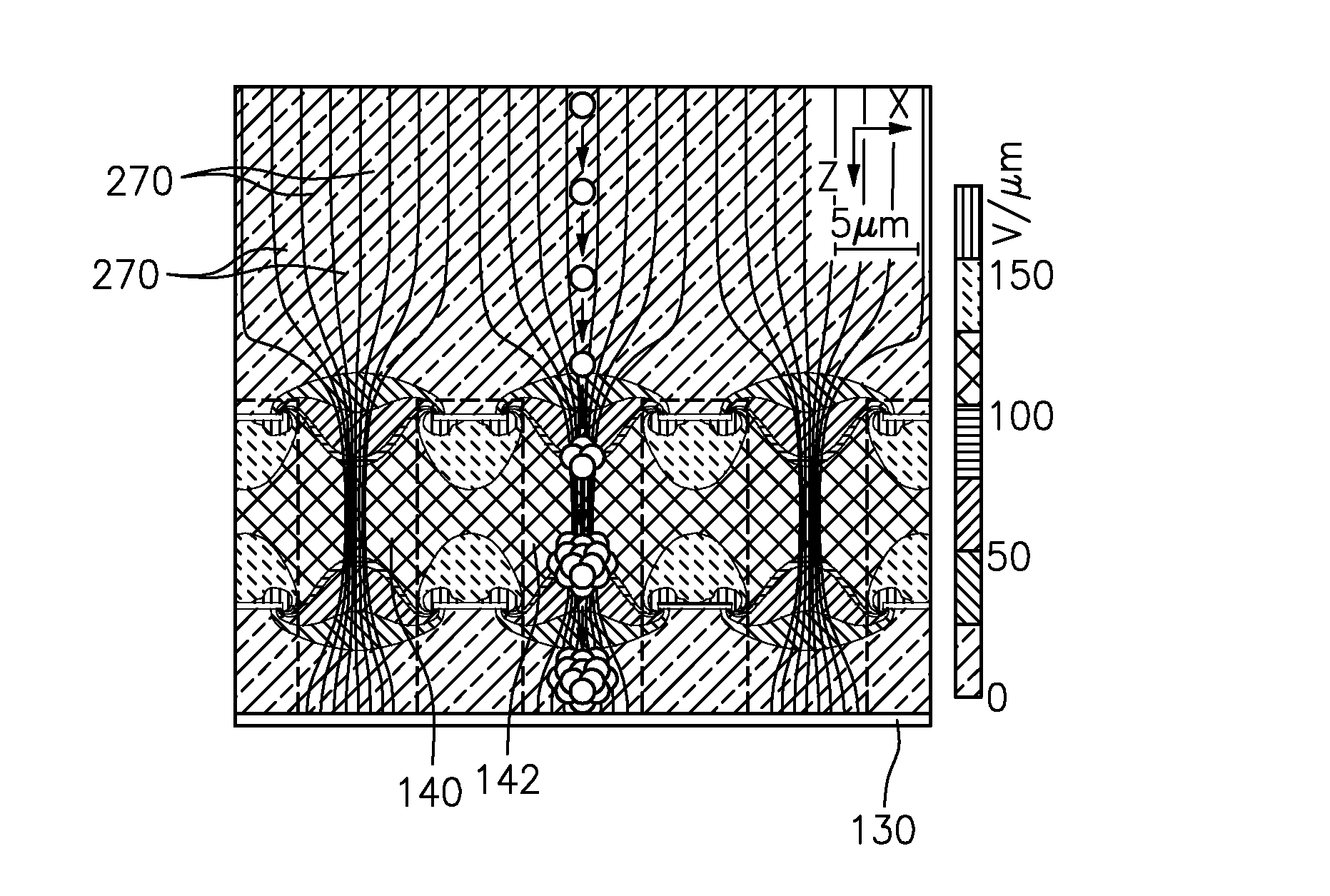
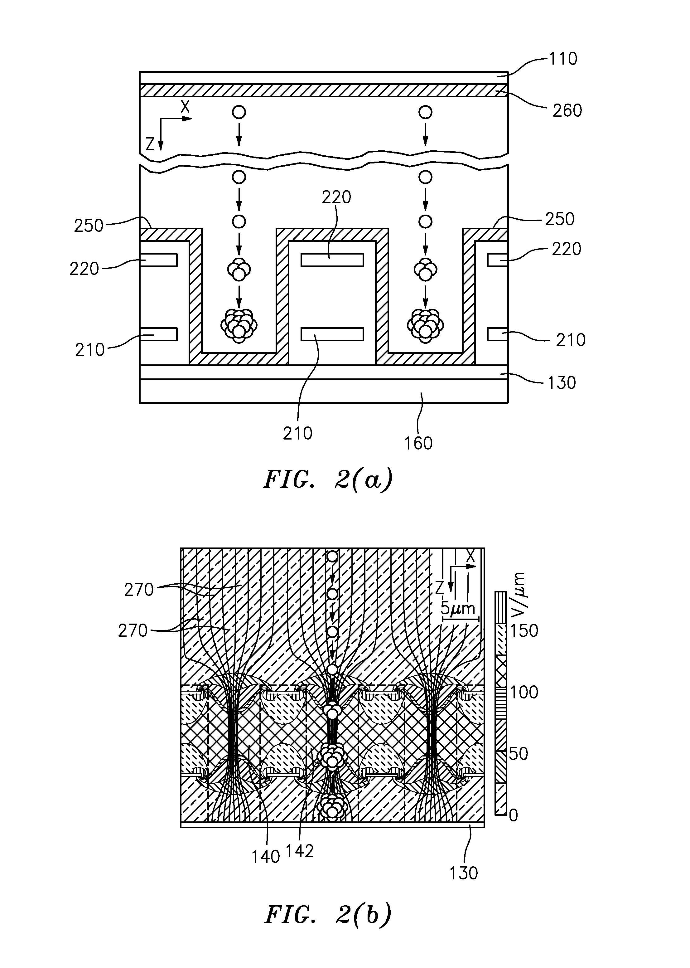
[0025]Disclosed herein is construction of a practical solid-state avalanche radiation detector using an amorphous material as the photoconductive layer that achieves stable and continuous avalanche multiplication gain using field-shaping inside each well, with the avalanche structure also referred to as a Multi-Well Solid-state Detector (MWSD).

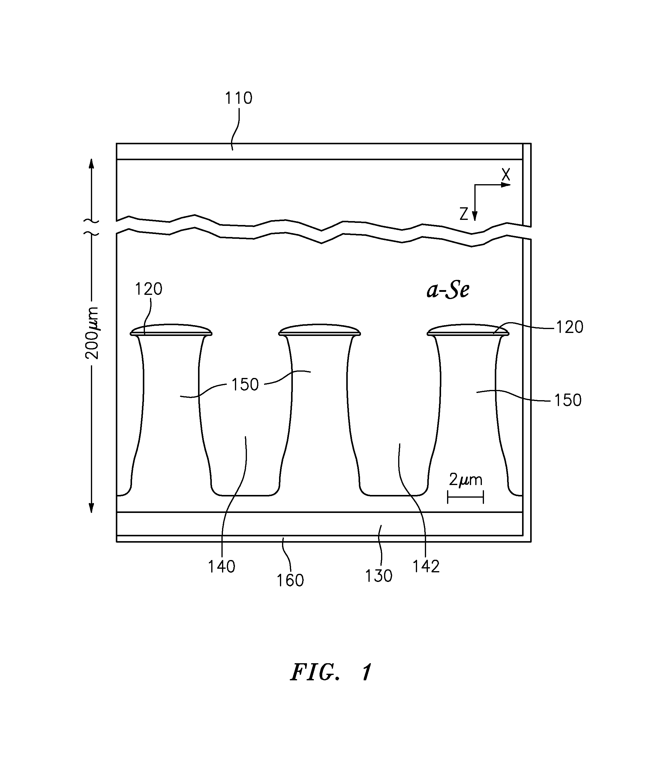
[0026]FIG. 1 is a Scanning Electron Microscope cross-section of a Micro Well Solid-state Detector (MWSD), showing a preferred arrangement of common electrode (110), shield (120), pixel electrode (130), a plurality of insulators (150) with a plurality of wells (14...


PUM

PropertyMeasurementUnit
electric fieldaaaaaaaaaa
widthaaaaaaaaaa
widthaaaaaaaaaa

Abstract

A field shaping multi-well avalanche detector and method for fabrication thereof are disclosed. The field shaping multi-well avalanche detector provides stable avalanche multiplication gain in direct conversion amorphous selenium radiation detectors. The detector provides stable avalanche multiplication gain by eliminating field hot-spots using high-density avalanche wells with insulated wells and field-shaping within each well.

Description

PRIORITY[0001]This application claims priority to U.S. Provisional Patent Application No. 61 / 673,484 filed with the U.S. Patent and Trademark Office on Jul. 19, 2012, the content of which is incorporated herein by reference.GOVERNMENT SUPPORT[0002]This invention was made with government support under grant number EB002655 awarded by the National Institute of Health. The government has certain rights in the invention.BACKGROUND OF THE INVENTION[0003]1. Field of the Invention[0004]The present invention relates generally to solid-state imaging detectors of ionizing radiation and, in particular, to amorphous selenium radiation detectors having a field-shaping multi-well avalanche detector structure.[0005]2. Description of the Related Art[0006]Soon after the Nobel Prize winning invention of the gas-filled multi-wire proportional chamber by Charpak in 1968 and parallel to developments in microelectronics, micro-pattern gaseous detectors were developed for improved position resolution. How...

Claims


Application Information

Patent Timeline
Patent Type & Authority Applications(United States)
IPC IPC(8): H01L31/0272H01L31/115H01L31/0376
CPCH01L31/0272H01L31/115H01L31/0376H01L31/107H01L27/14603
Inventor GOLDMAN, AMIRHOSSEINZHAO, WEI
Owner THE RES FOUND OF STATE UNIV OF NEW YORK
Why Eureka
Try Eureka