Liquid-crystal display device

a display device and liquid crystal technology, applied in non-linear optics, instruments, optics, etc., can solve problems such as deterioration of afterimages

Active Publication Date: 2015-07-02
TIANMA MICRO ELECTRONICS CO LTD
View PDF3 Cites 9 Cited by
  • Summary
  • Abstract
  • Description
  • Claims
  • Application Information

AI Technical Summary

Benefits of technology

[0021]IPS mode pixel comb electrodes and common comb electrodes are allowed to be structurally symmetrical, whereby the manners of emitting light between frames also become symmetrical, and signals applied between the pixel comb electrodes and the common comb electrodes also become symmetrical after a common potential is swung to perform flicker adjustment so that luminances are equivalent between frames. Therefore, an afterimage is improved.

Problems solved by technology

Therefore, an afterimage is considered to be deteriorated.

Method used


Image

  • Liquid-crystal display device
  • Liquid-crystal display device
  • Liquid-crystal display device

Examples


example 1

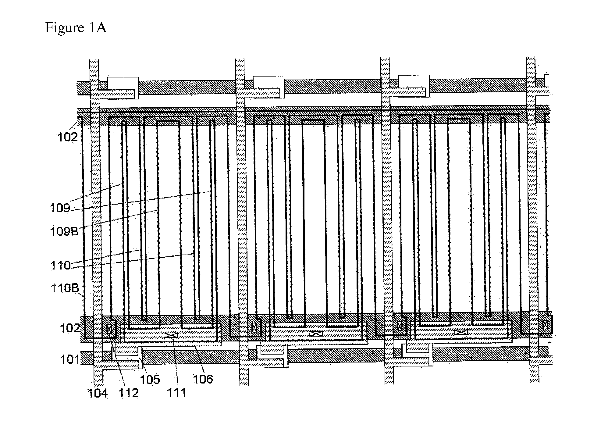
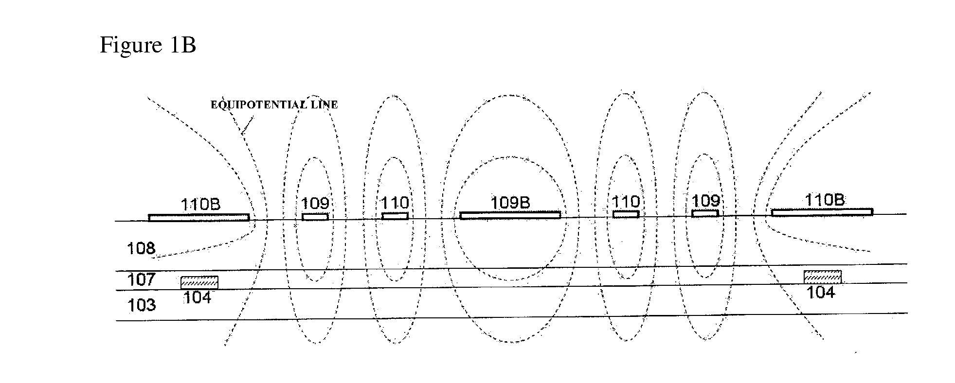
[0038]A first example of the present invention will be explained with reference to FIGS. 1(a), (b), and (c). FIG. 1A is a plan view of a liquid crystal display device according to the first example of the present invention, and FIG. 1B is a schematic view of the cross section and electric potential distribution of a display region. FIG. 1C is a cross-sectional view, in which a first substrate and a second substrate are allowed to face each other and to narrowly hold a liquid crystal layer.

[0039]More specifically, the lateral-electric-field mode active matrix liquid crystal display device of the present invention comprises: a first glass substrate 118 which is the first substrate; a second glass substrate 119 which is the second substrate facing the first substrate; and a liquid crystal layer 122 held in the state of being sandwiched between the first glass substrate 118 and the second glass substrate 119.

[0040]Example 1 formed as above is an example in which the number of columns is...

example 2

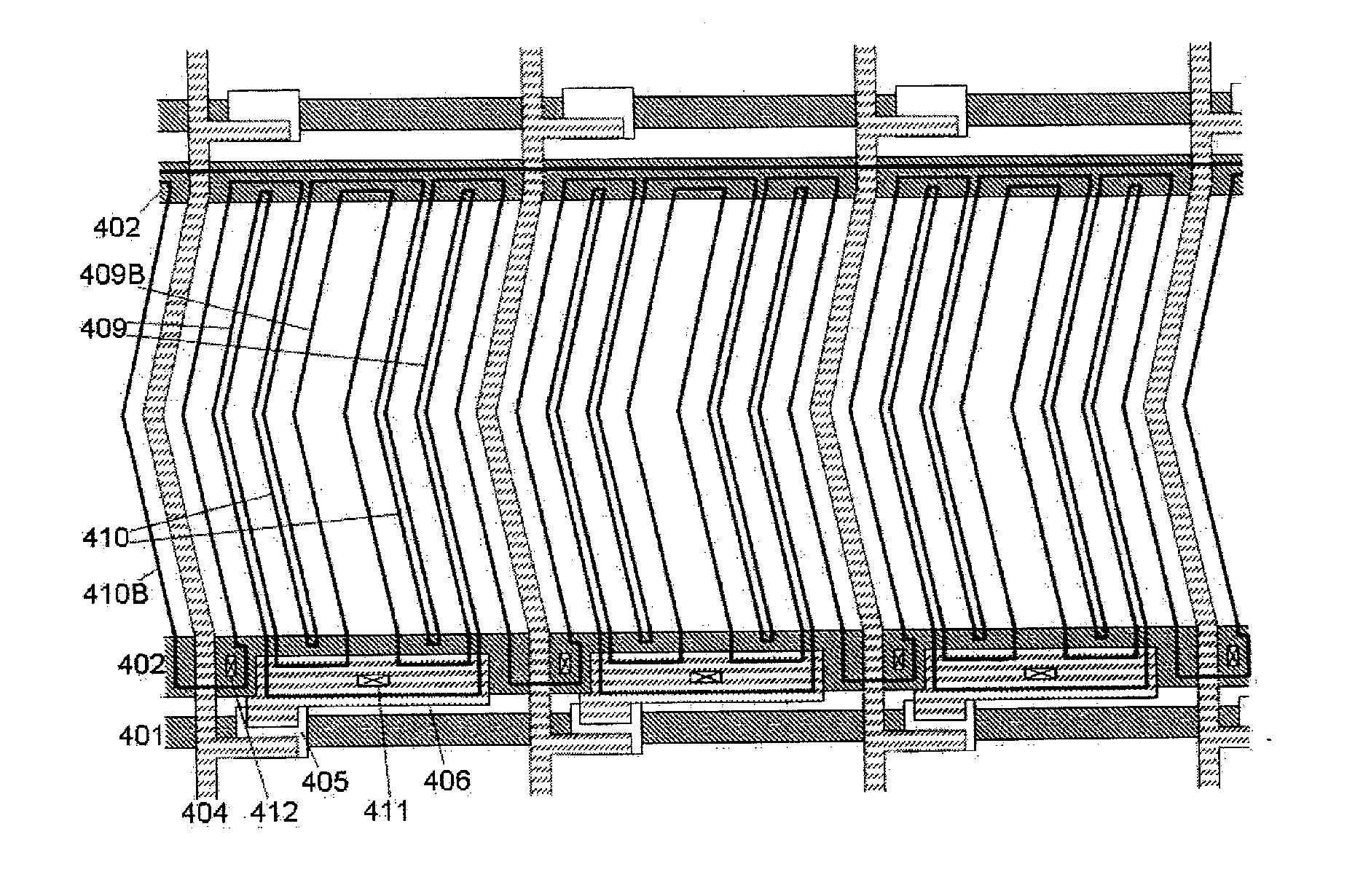
[0056]A second example of the present invention will be explained with reference to FIGS. 2(a) and (b). FIG. 2A is a plan view of a liquid crystal display device according to the second example of the present invention, and FIG. 2B is a schematic view of the cross section and electric potential distribution of a display region. The cross-sectional view is similar to that in the first example.

[0057]The difference from the first example is in that a common signal wiring line is formed underneath and in parallel with a pixel comb electrode 209B. The common signal wiring line is formed integrally with two common signal wiring lines 202 parallel to a scanning signal wiring line 201.

[0058]The wide pixel comb electrode 209B and each common signal wiring line 202 overlap one another, whereby a storage capacitance can be formed in this region.

[0059]The display region is divided into two subregions by the central widest pixel comb electrode 209B. In each subregion, the number of pixel comb el...

example 3

[0064]A third example of the present invention will be explained with reference to FIGS. 3(a) and (b). FIG. 3A is a plan view of a liquid crystal display device according to the third example of the present invention, and FIG. 3B is a schematic view of the cross section and electric potential distribution of a display region. The cross-sectional view is similar to that in the first example.

[0065]The difference from the second example is in that a common signal wiring line is formed underneath and in parallel with a wide pixel comb electrode 309B, and in addition, a source electrode 306 comprising a second metal layer is further extensionally formed underneath and in parallel with the wide pixel comb electrode 309B.

[0066]A common signal wiring line 302 and the source electrode 306 overlap one another underneath the wide pixel comb electrode 309B, whereby a storage capacitance can be formed in this region.

[0067]The display region is divided into two subregions by the wide pixel comb e...


PUM

PropertyMeasurementUnit
transparent conductiveaaaaaaaaaa
widthaaaaaaaaaa
electric fieldaaaaaaaaaa

Abstract

Provided is a lateral-electric-field mode active matrix liquid crystal display device in which an afterimage can be improved. The width of one pixel comb electrode 109B of a plurality of pixel comb electrodes 109 is larger than each of the widths of the other pixel comb electrodes 109 and common comb electrodes 110 and is equivalent to the width of a common shield electrode 110B that covers an image signal wiring line 104 via a second insulating film. A display region is divided into two subregions by the wide pixel comb electrode 109B. In each subregion, the number of pixel comb electrodes 109 is equal to that of common comb electrodes 110. In addition, the width of the common shield electrode 110B is equivalent to that of the wide pixel comb electrode 109B, and the concentration of an electric field in the vicinity of each pixel comb electrode is reduced. Since structural symmetry is achieved, an electric potential distribution becomes symmetrical, and the asymmetry of the manners of emitting light between frames is reduced. As a result, the DC offset component of an image signal after flicker adjustment is reduced to improve an afterimage.

Description

TECHNICAL FIELD[0001]The present invention relates to liquid crystal display devices and particularly relates to a lateral-electric-field mode active matrix liquid crystal display device having an excellent afterimage characteristic.BACKGROUND ART[0002]In an IPS (In-Plane Switching) mode, which has been broadly adopted for large-scale monitors in recent years, the molecular axis of a liquid crystal is rotated by in-plane switching in a plane parallel to a substrate, to produce a display. Thus, visual angle dependency on the rising angle of the molecular axis is precluded, and therefore, the visual angle characteristic of the IPS mode is greatly more advantageous than that of a TN mode. In contrast, since pixel electrodes and common electrodes are placed in a comb form to apply a lateral electric field in the IPS mode, the rate of the area of the electrodes to a display region becomes high. Thus, an opening ratio in the IPS mode has been considered to be more disadvantageous than tha...

Claims


Application Information

Patent Timeline
Patent Type & Authority Applications(United States)
IPC IPC(8): G02F1/1343G02F1/1362G02F1/1368
CPCG02F1/134363G02F1/1368G02F2001/136218G02F1/13439G02F1/134309G02F1/136286G02F1/136218
Inventor KONNO, TAKAYUKI
Owner TIANMA MICRO ELECTRONICS CO LTD
Why Eureka
Try Eureka