Organic light emitting diode display device with touch screen and method of fabricating the same

a technology of light-emitting diodes and display devices, which is applied in the direction of static indicating devices, solid-state devices, instruments, etc., can solve the problems of increasing design constraints in the final product, and achieve the effects of reducing the number of components and manufacturing costs, light weight, and thin profil

Active Publication Date: 2015-07-02
LG DISPLAY CO LTD
View PDF8 Cites 129 Cited by
  • Summary
  • Abstract
  • Description
  • Claims
  • Application Information

AI Technical Summary

Benefits of technology

[0015]An object of the present disclosure is to provide an organic light emitting diode display device with a touch screen and a method of fabricating the same that decrease the number of components and manufacturing costs and have light weight and a thin profile.

Problems solved by technology

Therefore, the multiple FPC connectors 99a and 99b increase constraints in designing the final product.

Method used


Image

  • Organic light emitting diode display device with touch screen and method of fabricating the same
  • Organic light emitting diode display device with touch screen and method of fabricating the same
  • Organic light emitting diode display device with touch screen and method of fabricating the same

Examples


first embodiment

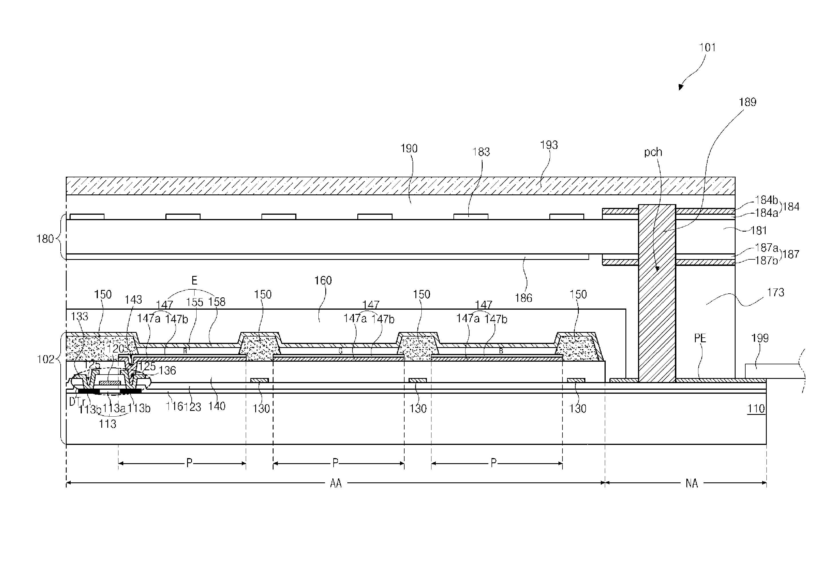
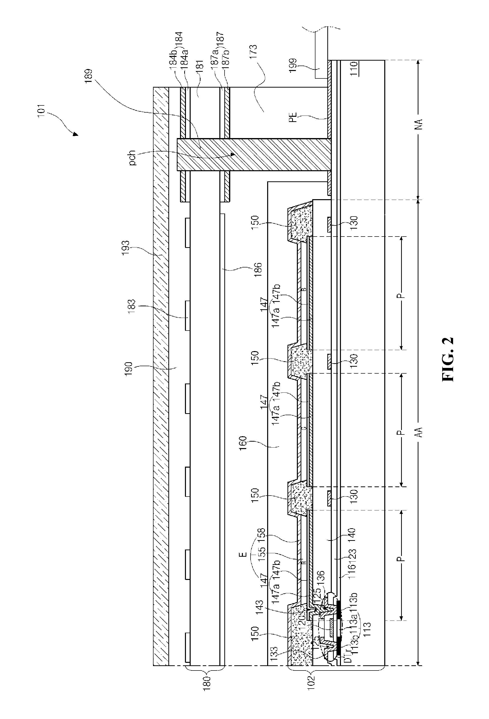
[0028]FIG. 2 is a cross-sectional view of an OLED display device 101 with a touch screen 180 according to the present invention. For convenience of explanation, a display area AA and a non-display area NA are defined. An image is displayed in the display area AA, and a plurality of first pads (not shown) and a plurality of second pads PE are disposed in the non-display area NA at the outside of the display area AA.

[0029]In FIG. 2, an OLED display device 101 with a touch screen 180 according to the first embodiment includes a display panel 102, an encapsulation film 160, and a touch screen 180. The display panel 102 is an OLED panel and includes a switching thin film transistor (not shown), a driving thin film transistor DTr, and an organic light emitting diode E in each pixel region P. The organic light emitting diodes E in the pixel regions P sequentially emit red, green, and blue light. The encapsulation film 160 protects the organic light emitting diodes E. The touch screen 180 i...

second embodiment

[0106]FIG. 5 is a cross-sectional view of an OLED display device 105 with a touch screen according to a

[0107]A touch screen of the OLED display device 105 according to the second embodiment is an in-cell type and is disposed on an inner surface of a substrate 202 of an encapsulation panel 210 opposite to a display panel 102 with organic light emitting diodes E. The encapsulation panel 210 includes a color filter layer 182.

[0108]In addition, the display panel 102 of the second embodiment has substantially the same structure as the display panel 102 of FIG. 2 of the first embodiment except that the organic light emitting diodes E of the display panel 102 according to the second embodiment emit white light and an organic light emitting layer 155 of the second embodiment is formed substantially all over a display area AA. Accordingly, explanation of the same parts as the display panel 102 of FIG. 2 of the first embodiment is omitted.

[0109]A black matrix 181 is formed on the inner surfac...


PUM


Abstract

An OLED display device with a touch screen includes first and second substrates; organic light emitting diodes in the display area over the first substrate; first pads and second pads in the non-display area over the first substrate; first and second touch electrodes in the display area over the second substrate; touch pads in the non-display area over the second substrate and corresponding to and overlapping the second pads, respectively; and a first adhesive layer between the first and second substrates and exposing the first and second pads, wherein pad contact holes pass through the second substrate, the touch pads, and the first adhesive layer and expose the second pads, respectively, and wherein a conduction means is disposed in each of the pad contact holes and electrically connects each of the touch pads with a corresponding second pad.

Description

CROSS-REFERENCE TO RELATED APPLICATION[0001]The present application claims the priority benefit of Korean Patent Application No. 10-2013-0163901 filed in the Republic of Korea on Dec. 26, 2013, which is hereby incorporated by reference in its entirety.BACKGROUND[0002]1. Field of the Disclosure[0003]The present disclosure relates to an organic light emitting diode display device with a touch screen, and more particularly, to an organic light emitting diode display device with a touch screen in which a display panel and a touch screen are connected to an external driving circuit board via a flexible printed circuit board (FPC) connector and a method of fabricating the same.[0004]2. Discussion of the Related Art[0005]Organic light emitting diode (OLED) display devices of flat panel displays, which may be referred to as organic electroluminescent display devices, have high brightness and low driving voltages. In addition, because they are self-luminous, OLED display devices have excelle...

Claims


Application Information

Patent Timeline
Patent Type & Authority Applications(United States)
IPC IPC(8): G06F3/041H01L51/56H01L27/32
CPCG06F3/0412H01L27/323H01L27/3276G06F2203/04103H01L27/322H01L51/56H01L27/3248G06F3/0445G06F3/04164H10K59/40G06F3/041H10K59/00
Inventor KIM, HYOUNG-SULEE, BU-YEOL
Owner LG DISPLAY CO LTD
Why Eureka
Try Eureka