Flexible display device and method for fabricating the same
a display device and flexible technology, applied in the field of flexible display devices, can solve the problems of wire short circuit, wire short circuit, wire short circuit, etc., and achieve the effect of preventing wire short circuit or disconnection
- Summary
- Abstract
- Description
- Claims
- Application Information
AI Technical Summary
Benefits of technology
Problems solved by technology
Method used
Image
Examples
first embodiment
[0053]FIG. 4 is a planar view of a flexible organic light-emitting diode (OLED) display device according to the present invention.
[0054]Referring to FIG. 4, the flexible OLED display device 100 according to a first embodiment of the present invention may be formed on a flexible substrate 110 including an active area (display area) (A / A) and a non-active area (non-display area) (N / A).
[0055]The active area (A / A) is a region where an image is substantially displayed. On the active area (A / A), a plurality of gate lines (GL) and a plurality of data lines (DL) may be formed to cross each other, thereby defining pixel regions. A plurality of sensing lines (SL) may be formed in parallel to the plurality of gate lines (GL).
[0056]Power lines for supplying a driving voltage (VDD), a reference voltage (Vref) and a ground voltage (GND) to pixel regions, e.g., a driving voltage line 146b, a reference voltage line 147b and a ground line 145b may be formed in the active area (A / A).
[0057]A pixel (P)...
second embodiment
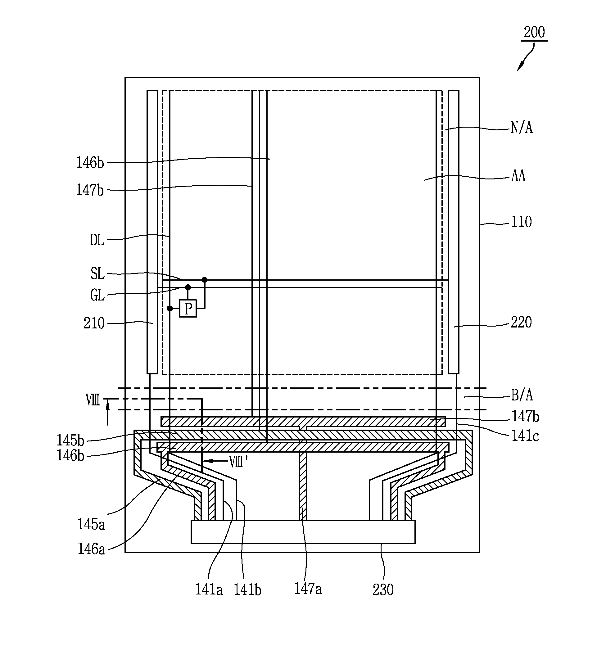
[0139]FIG. 8 is a planar view of a flexible OLED display device according to the present invention.
[0140]Referring to FIG. 8, the flexible OLED display device according to the second embodiment may be formed on a flexible substrate 110 having an active area (A / A) and a non-active area (N / A).
[0141]The active area (A / A) is a region where an image is substantially displayed. On the active area (A / A), a plurality of gate lines (GL) and a plurality of data lines (DL) may be formed to cross each other, thereby defining pixel regions. A plurality of sensing lines (SL) may be formed in parallel to the plurality of gate lines (GL).
[0142]Power lines for supplying a driving voltage (VDD), a reference voltage (Vref) and a ground voltage (GND) to pixel regions, e.g., a driving voltage line 146b, a reference voltage line 147b and a ground line 145b may be formed in the active area (A / A).
[0143]A pixel (P) having a plurality of switching devices may be formed at the pixel region. The pixel (P) may ...
PUM
 Abstract
Description
Claims
Application Information


