Semiconductor memory device and method of operating the same

a memory device and semiconductor technology, applied in static storage, digital storage, instruments, etc., can solve the problems of inadequate threshold voltage distribution and data stored in the ram, and achieve the effect of improving the threshold voltage distribution of memory cells after an erase operation of the semiconductor memory devi

Active Publication Date: 2015-07-30
SK HYNIX INC
View PDF4 Cites 2 Cited by
  • Summary
  • Abstract
  • Description
  • Claims
  • Application Information

AI Technical Summary

Benefits of technology

[0013]Various embodiments are provided for a semiconductor memory device for improving threshold voltage distribution of memory cells after an erase operation of the semiconductor memory device is performed and a method of operating the same.
[0018]In an embodiment, threshold voltage distribution of memory cells after an erase operation of the semiconductor memory device may be performed may be improved.

Problems solved by technology

Data stored in the RAM becomes lost if power is not supplied.
However, in case that every memory cell is simultaneously programmed through FN tunneling method, threshold voltage of every memory cell increases, and so effect of reducing width of the threshold voltage distribution is inadequate.

Method used


Image

  • Semiconductor memory device and method of operating the same
  • Semiconductor memory device and method of operating the same
  • Semiconductor memory device and method of operating the same

Examples


Embodiment Construction

[0026]Hereinafter, the various embodiments will be explained in more detail with reference to the accompanying drawings. Although embodiments have been described with reference to a number of illustrative embodiments thereof, it should be understood that numerous other modifications and embodiments can be devised by those skilled in the art that will fall within the spirit and scope of the principles of this disclosure.

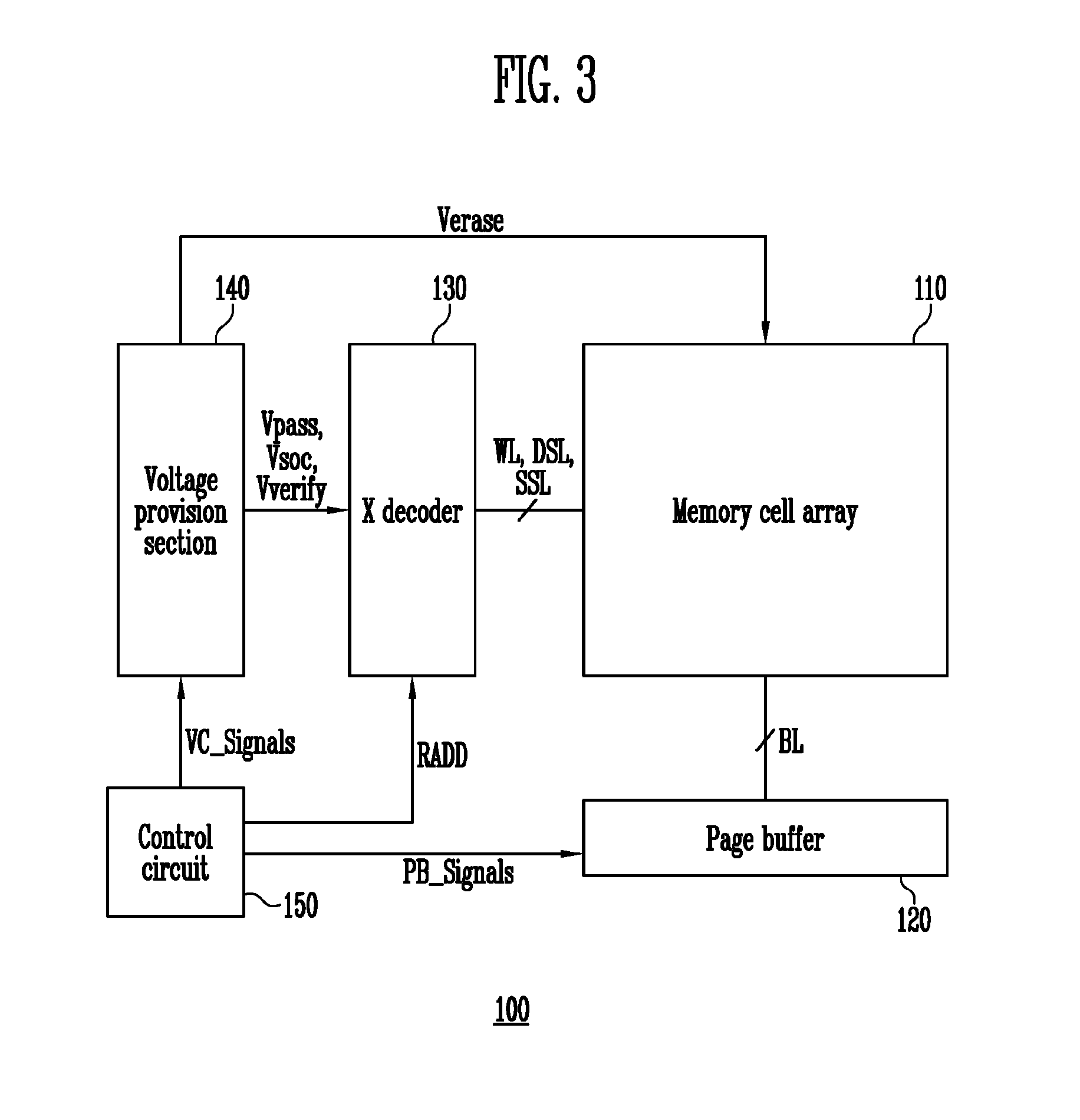
[0027]FIG. 3 is a block diagram illustrating a semiconductor memory device according to an embodiment.

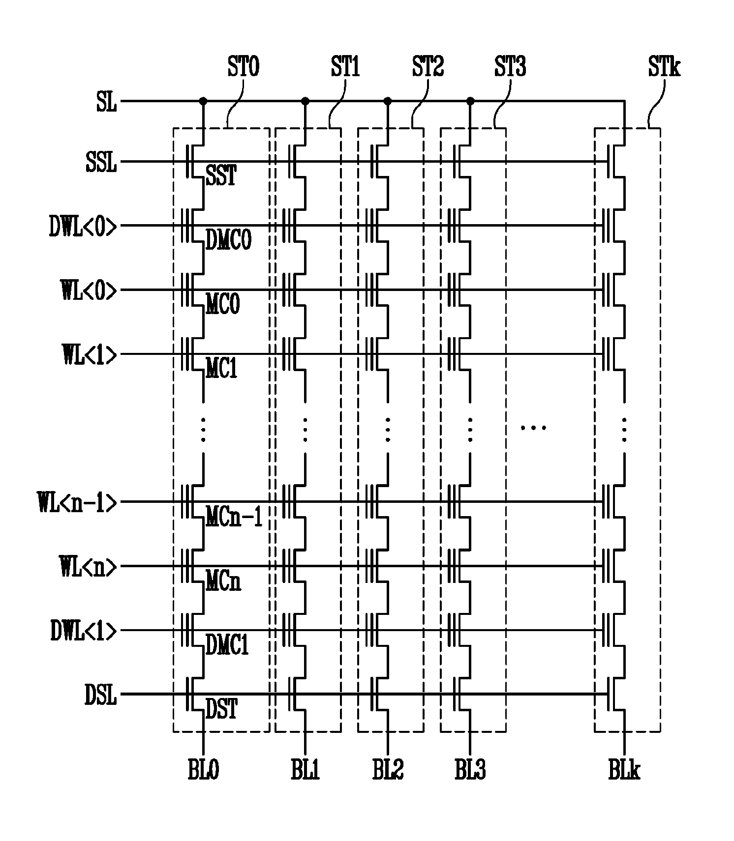
[0028]In FIG. 3, the semiconductor memory device 100 may include a memory cell array 110, a page buffer 120, an X decoder 130, a voltage provision section 140 and a control circuit 150.

[0029]The memory cell array 110 may include memory cells. Detailed constitution of the memory cell array will be described below.

[0030]The page buffer 120 may be connected to bit lines BL of the memory cell array 110. The page buffer 120 senses the potentials of the bit lines BL in resp...


PUM


Abstract

A semiconductor memory device and a method of operating the same are disclosed. The semiconductor memory device includes a memory cell array configured to include memory cells, a peripheral circuit configured to perform an erase operation and a soft program operation and a control circuit configured to control the peripheral circuit so that the memory cells are programmed though a hot carrier injection HCI method when the soft program operation is performed.

Description

CROSS-REFERENCE TO RELATED APPLICATION[0001]This application claims priority from Korean Patent Application No. 10-2012-0093161, filed on Aug. 24, 2012, the contents of which are incorporated herein by reference in its entirety.BACKGROUND[0002]1. Technical Field[0003]The present invention generally relates to a semiconductor memory device and method of operating the same, more particularly relates to a semiconductor memory device for performing a soft program operation after an erase operation is performed and method of operating the same.[0004]2. Related Art[0005]A semiconductor memory device is a memory device for enabling to store and read data. The semiconductor memory device is divided into a random access memory RAM and a read only memory ROM. Data stored in the RAM becomes lost if power is not supplied. This memory is referred to as a volatile memory. However, data stored in ROM is not lost though the power is not supplied. This memory is referred to as non-volatile memory.[0...

Claims


Application Information

Patent Timeline
Patent Type & Authority Applications(United States)
IPC IPC(8): G11C16/14G11C16/34
CPCG11C16/14G11C16/3459G11C16/3445G11C16/0483G11C16/10G11C16/34
Inventor JANG, YOON SOO
Owner SK HYNIX INC
Why Eureka
Try Eureka