Substrate-type waveguide element and optical modulator

a waveguide element and waveguide technology, applied in the direction of optical waveguide light guides, optical fibres with multi-layer cores/claddings, instruments, etc., can solve the problems of increasing device size and production costs, not being able to avoid losing a tmb>0/b> polarized wave, etc., to achieve the effect of increasing decreasing a polarization extinction ratio

Active Publication Date: 2015-08-20
THE FUJIKURA CABLE WORKS LTD
View PDF2 Cites 0 Cited by
  • Summary
  • Abstract
  • Description
  • Claims
  • Application Information

AI Technical Summary

Benefits of technology

[0031]With the present invention, it is possible to (i) increase a polarization extinction ratio without increasing loss of a TM polarized wave having a wavelength outside a design wavelength or (ii) decrease, without decreasing a polarization extinction ratio, loss of a TM polarized wave having a wavelength outside a design wavelength.

Problems solved by technology

However, in a case where polarization-division multiplexing is carried out, a configuration of an optical modulator becomes complex.
This results in problems such as increases in device size and production costs.
Therefore, it is not possible to avoid losing a TM0 polarized wave having a wavelength outside the design wavelength.

Method used


Image

  • Substrate-type waveguide element and optical modulator
  • Substrate-type waveguide element and optical modulator
  • Substrate-type waveguide element and optical modulator

Examples


example

[0076]The following description will discuss, with reference to FIGS. 3 through 5, an example of the substrate-type waveguide element 1 in accordance with the present embodiment.

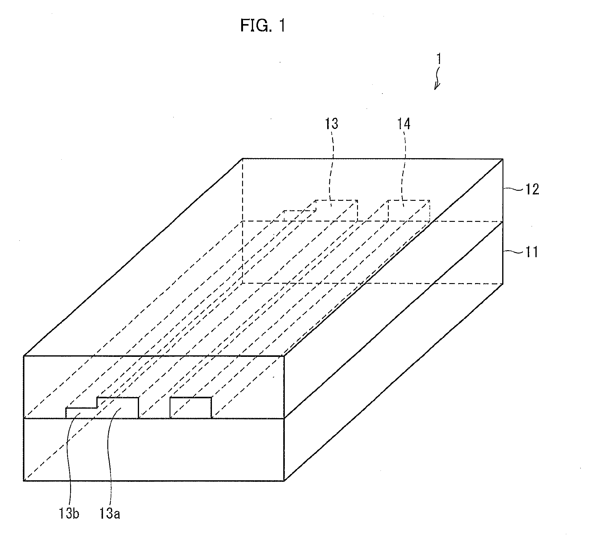
[0077](a) of FIG. 3 is a plan view of a substrate-type waveguide element 1 in accordance with the example. (b) of FIG. 3 is a cross-sectional view of the substrate-type waveguide element 1.

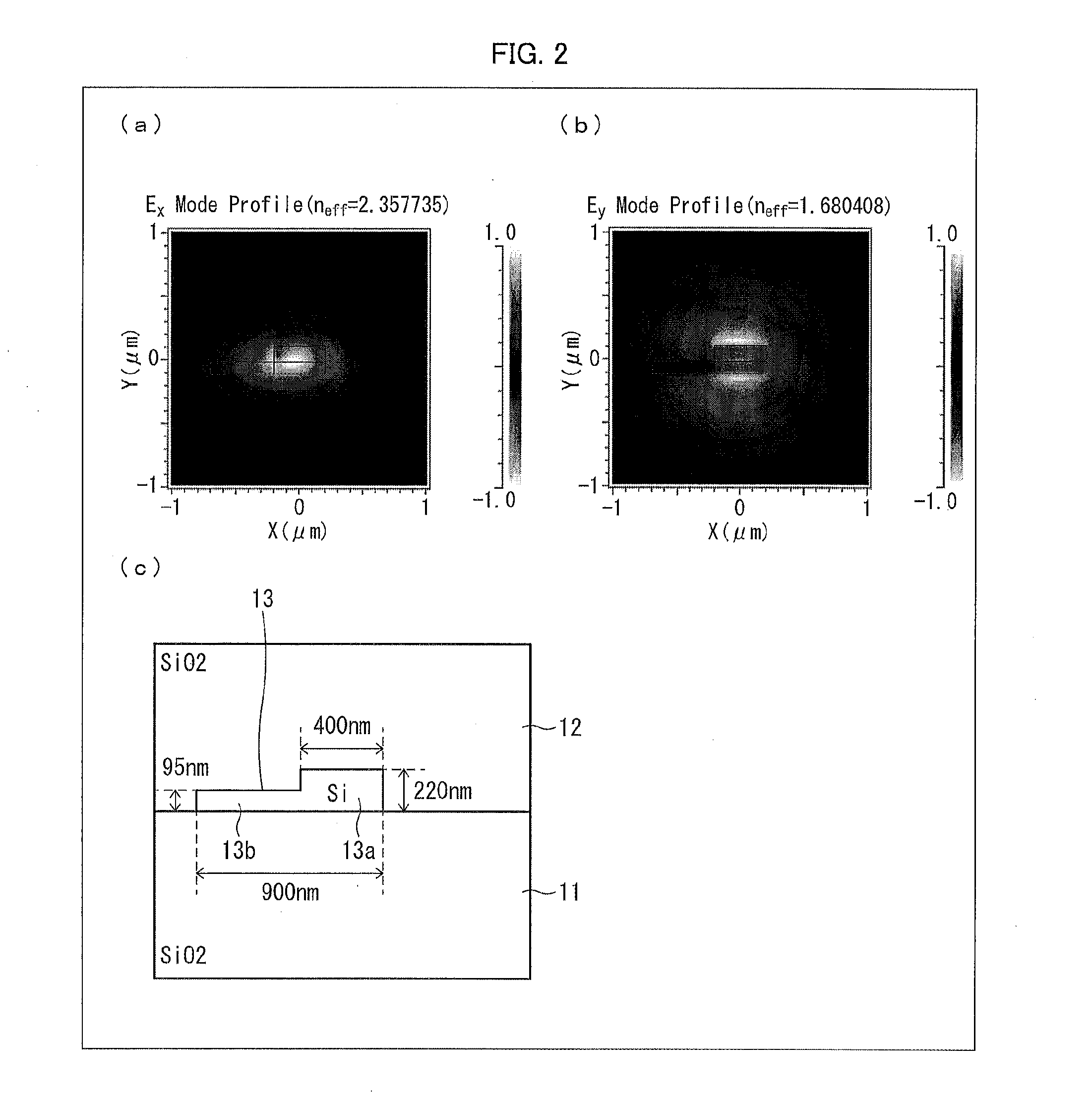
[0078]In the present example, cross-sectional shapes of two cores 13 and 14 included in the substrate-type waveguide element 1 were designed in the following steps. First, the cross-sectional shape of the first core 13 was determined to be a step-like shape as illustrated in (b) of FIG. 3. Then, an effective refractive index N1 of a TM0 polarized wave, which had a wavelength of 1580 nm and which was guided through the first core 13, was calculated, and was determined to be 1.68041. Then, a height of the second core 14 was configured to be 220 nm (which is equal to a height of a main part 13a of the first core 13). Then, an...


PUM


Abstract

Since a cross section of at least a partial segment of a first core has a step-like shape including a quadrilateral shape of a main part and a quadrilateral shape of a protruding part protruding from the main part, respective effective refractive indices of TE polarized waves in the first core and in the second core differ from each other.

Description

[0001]This Nonprovisional application claims priority under 35 U.S.C. §119 on Patent Application No. 2014-027743 filed in Japan on Feb. 17, 2014, the entire contents of which are hereby incorporated by reference.TECHNICAL FIELD[0002]The present invention relates to (i) a substrate-type waveguide element configured such that a TM polarized wave inputted from a first core is outputted from a second core and (ii) an optical modulator including the substrate-type waveguide element.BACKGROUND ART[0003]The amount of information to be transmitted via optical communication is steadily increasing. In order to match up to such an increase in the amount of information, attempts are being made such as an increase in signal speed and an increase in the number of channels by wavelength-division multiplexing. A next-generation 100-Gbps digital coherent transmission technology which is intended for high-speed information communication, in particular, attempts to double the amount of information to ...

Claims


Application Information

Patent Timeline
Patent Type & Authority Applications(United States)
IPC IPC(8): G02B6/10G02B6/036
CPCG02B6/036G02B6/105G02B6/2773G02B2006/12147G02F1/3133G02F2201/063G02F2202/105G02F2203/06G02B6/126G02B6/0048
Inventor OKA, AKIRA
Owner THE FUJIKURA CABLE WORKS LTD
Why Eureka
Try Eureka