Organic Optoelectronic Component and Method for Operating the Organic Optoelectronic Component

an optoelectronic component and organic technology, applied in the direction of electroluminescent light sources, electroluminescent devices, electric lighting sources, etc., can solve the problems of reducing the luminance, requiring a high complexity, and damage to organic materials, so as to improve the incident light intensity and the effect of low complexity

Active Publication Date: 2015-08-27
DOLYA HOLDCO 5 LTD
View PDF3 Cites 4 Cited by
  • Summary
  • Abstract
  • Description
  • Claims
  • Application Information

AI Technical Summary

Benefits of technology

[0025]As a result of the monolithic integration of the at least one organic light detecting element, which can have, for example, the same layer construction as the at least one organic light emitting element, on a preferably small, separated area region of the common substrate, in addition to the at least one organic light emitting element a sensor element can be integrated with low complexity in the organic optoelectronic component described here. Depending on the intensity of the light which is incident on the organic light detecting element and which is composed of the sum of all incident light sources, an electrically measurable signal such as, for instance, a photovoltage, a photocurrent or a resistance change is generated which, in terms of absolute value, turns out to be all the higher, the higher the incident light intensity. The sum of all incident light sources can be formed, for example, by scattered light—guided internally in the organic optoelectronic component—of the light emitted by the at least one organic light emitting element during operation, by externally reflected light, by light of other light sources and combinations thereof. The electrically measurable signal of the at least one organic light detecting element can be processed further in an electronic circuit which can be formed by an external electronic component or which can form a part of the organic optoelectronic component as a monolithic element. By means of the electronic circuit, the organic light emitting element can in turn be controlled such that the luminous intensity at the location of the at least one organic light detecting element can be kept constant. The area of the at least one organic light detecting element can be adapted such that a sufficiently stable electrical signal can be generated during operation, without an instability of the light source, that is to say of the at least one organic light emitting element, being brought about on account of unstable feedback.
[0026]In the case of the organic optoelectronic component described here, it may advantageously be possible to achieve an exact automatic readjustment of the emitted light intensity of the organic light emitting element without an external sensor, which can considerably reduce in particular the circuitry outlay in comparison with known solutions. In particular, the light emitting diode is kept constant automatically at the light originating location independently of ageing properties of the light source even under variable ambient conditions, wherein it is possible to make use of the fact, for example, that the at least one organic light detecting element ages significantly more slowly than the at least one organic light emitting element, since, in particular, the organic materials of the at least one organic light detecting element are subjected to less loading, in particular less thermal loading.

Problems solved by technology

The decrease in the luminance can be caused, for example, by elevated temperatures which can occur during operation and can damage the organic materials.
However, such a possibility usually requires a high complexity and causes additional costs.
Manual dimming, by contrast, enables only imprecise coordination with lighting conditions actually present and causes an unnecessary waste of energy and, under certain circumstances, incorrect illumination conditions.
Since the known control possibilities for surface light sources have a high interconnection complexity or cannot be automated, an automatic readjustment of the luminance is not possible without considerable additional outlay.

Method used


Image

  • Organic Optoelectronic Component and Method for Operating the Organic Optoelectronic Component
  • Organic Optoelectronic Component and Method for Operating the Organic Optoelectronic Component
  • Organic Optoelectronic Component and Method for Operating the Organic Optoelectronic Component

Examples


Embodiment Construction

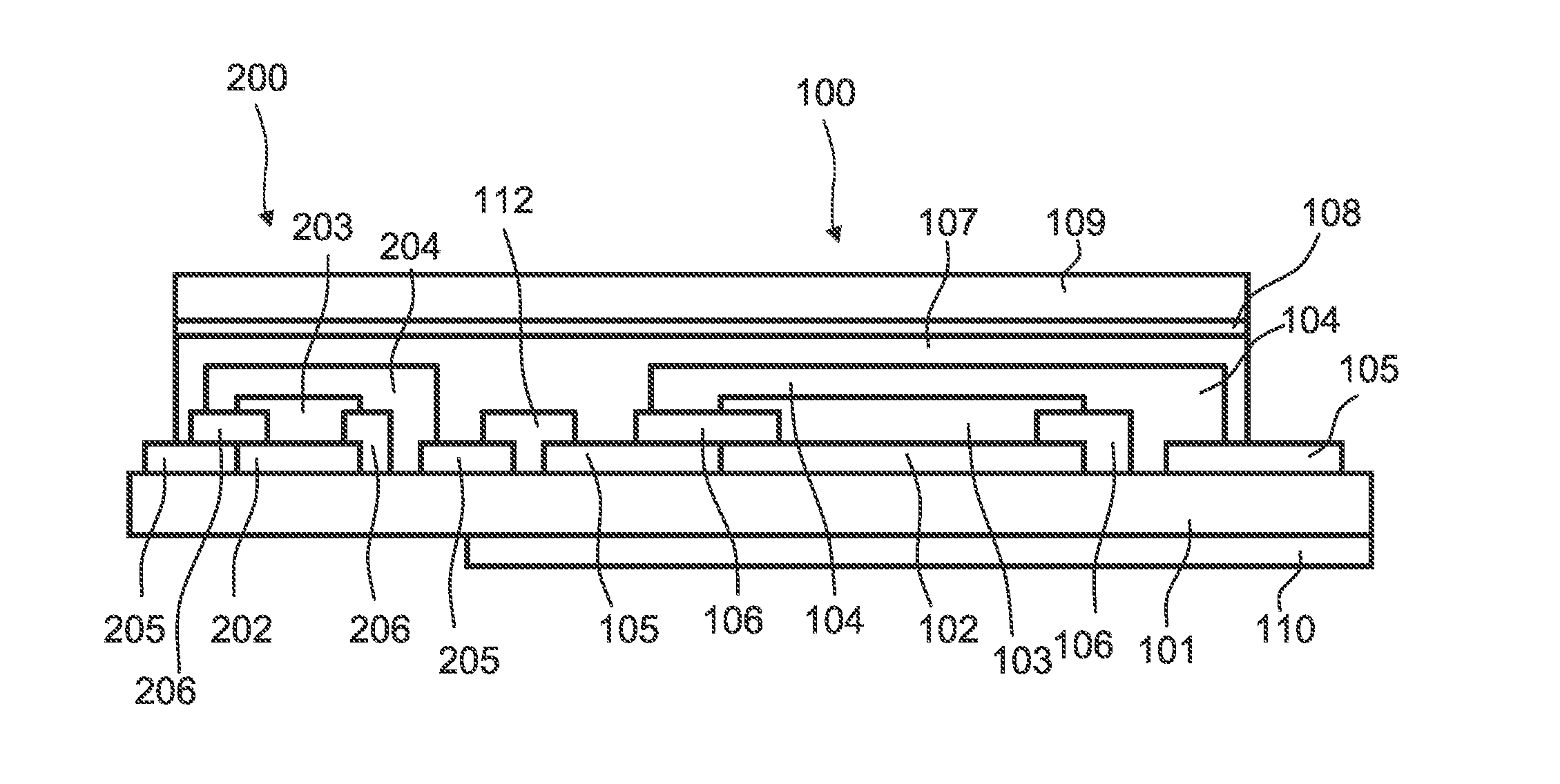
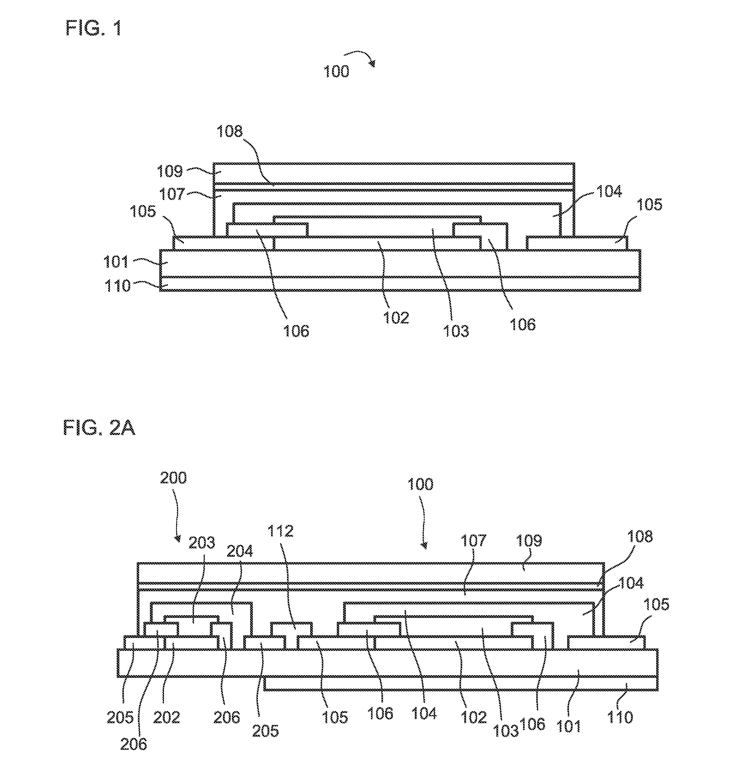
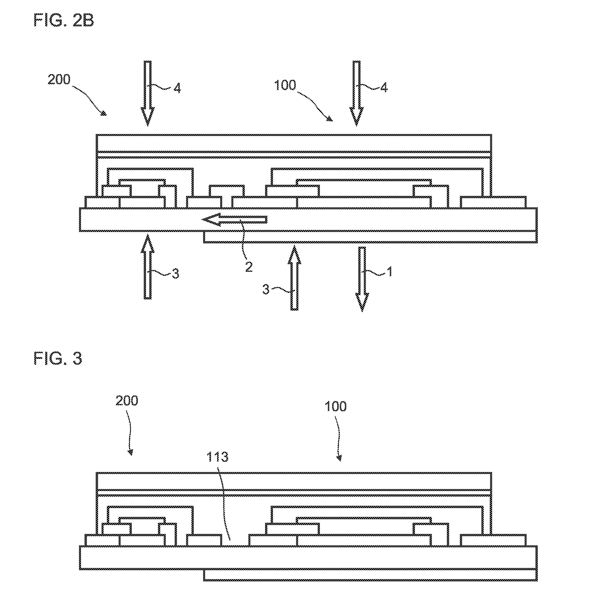
[0054]FIG. 1 shows in accordance with an embodiment the basic construction of an organic light emitting element 100 embodied as an organic light emitting diode (OLED).

[0055]The organic light emitting element 100, which may also be designated as OLED 100 hereinafter, comprises a substrate 101, on which an organic functional layer stack 103 having at least one organic light emitting layer is arranged between electrodes 102 and 104. At least one of the electrodes 102, 104 is embodied as transparent, such that light generated in the organic functional layer stack 103 during the operation of the OLED 100 can be radiated through the at least one transparent electrode.

[0056]In the OLED 100 shown in FIG. 1, the substrate 101 is embodied as transparent, for example, in the form of a glass plate or glass layer. As an alternative thereto, the substrate 101 can, for example, also comprise a transparent plastic or a glass-plastic laminate.

[0057]The electrode 102 applied on the substrate 101 is l...


PUM


Abstract

An organic optoelectronic component and a method for operating the organic optoelectronic component are disclosed. In an embodiment the organic optoelectronic component includes at least one organic light emitting element including an organic functional layer stack having at least one organic light emitting layer between two electrodes and at least one organic light detecting element including at least one organic light detecting layer, wherein the at least one organic light detecting element and the at least one organic light emitting element are laterally arranged on a common substrate.

Description

[0001]This patent application is a national phase filing under section 371 of PCT / EP2013 / 072318, filed Oct. 24, 2013, which claims the priority of German patent application 10 2012 220 020.7, filed Nov. 2, 2012, each of which is incorporated herein by reference in its entirety.TECHNICAL FIELD[0002]An organic optoelectronic component and a method for operating the organic optoelectronic component are specified.BACKGROUND[0003]In illuminated environments, changed ambient conditions can change the illumination conditions or brightnesses. By way of example, the ambient conditions can change with regard to the current illumination, which corresponds to short-term processes, and as a result of ageing processes in the luminance sources used, which corresponds to long-term processes. Changed ambient conditions with regard to the illumination arise, for example, in the case of changed light incidence through windows into an illuminated room at different times of day. Surface light sources su...

Claims


Application Information

Patent Timeline
Patent Type & Authority Applications(United States)
IPC IPC(8): H01L27/28H01L51/52H05B33/08H01L51/44H05B44/00
CPCH01L27/288H05B33/0896H01L51/5237H01L51/448Y02E10/549H10K65/00H10K50/8426H10K50/844H05B45/60H10K30/88H10K50/84
Inventor POPP, MICHAELPHILIPPENS, MARC
Owner DOLYA HOLDCO 5 LTD
Why Eureka
Try Eureka