Holey optical device

a technology of optical devices and holes, applied in the field of optical devices, can solve the problems of difficult fabrication process, tens of micrometer thickness, and non-uniform design of dielectric-based refraction microlenses typically used in optical systems, and achieve the effect of thin coating

Active Publication Date: 2015-09-03
PURDUE RES FOUND INC
View PDF12 Cites 17 Cited by
  • Summary
  • Abstract
  • Description
  • Claims
  • Application Information

AI Technical Summary

Problems solved by technology

Currently, dielectric-based refraction microlenses typically used in optical systems have a non-uniform design, with a thickness of tens of micrometers.
Gradient-index lenses are planar; however, their thicknesses are about an order of magnitude larger than the wavelength of incident light and the fabrication process is not straightforward.
Classical diffraction lenses, such as Fresnel lenses, are planar and thin; however, they cannot control the phases precisely because the position of each Fresnel ring is determined by the geometry.
Although nanoslit lenses are indeed planar and quite thin, an important drawback of the nanoslit design is its polarization-dependence.
Moreover, as a nanoslit lens is focusing light into a narrow strip, it does not allow for high-intensity confinement of light into a wavelength-size circular spot.
For some applications, the above features hinder the reduction of nanoslit lenses to practice.

Method used


Image

  • Holey optical device
  • Holey optical device
  • Holey optical device

Examples


Embodiment Construction

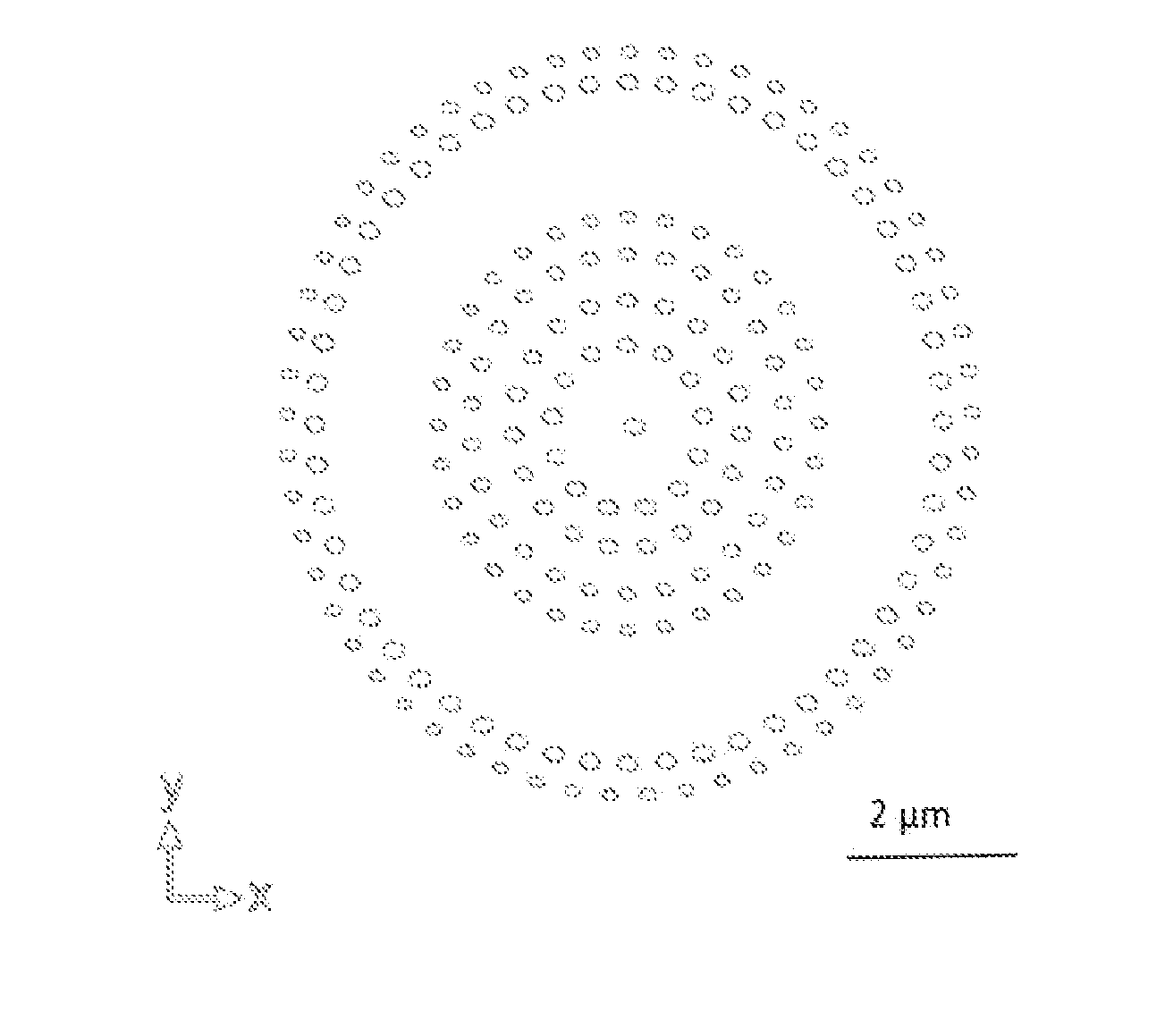
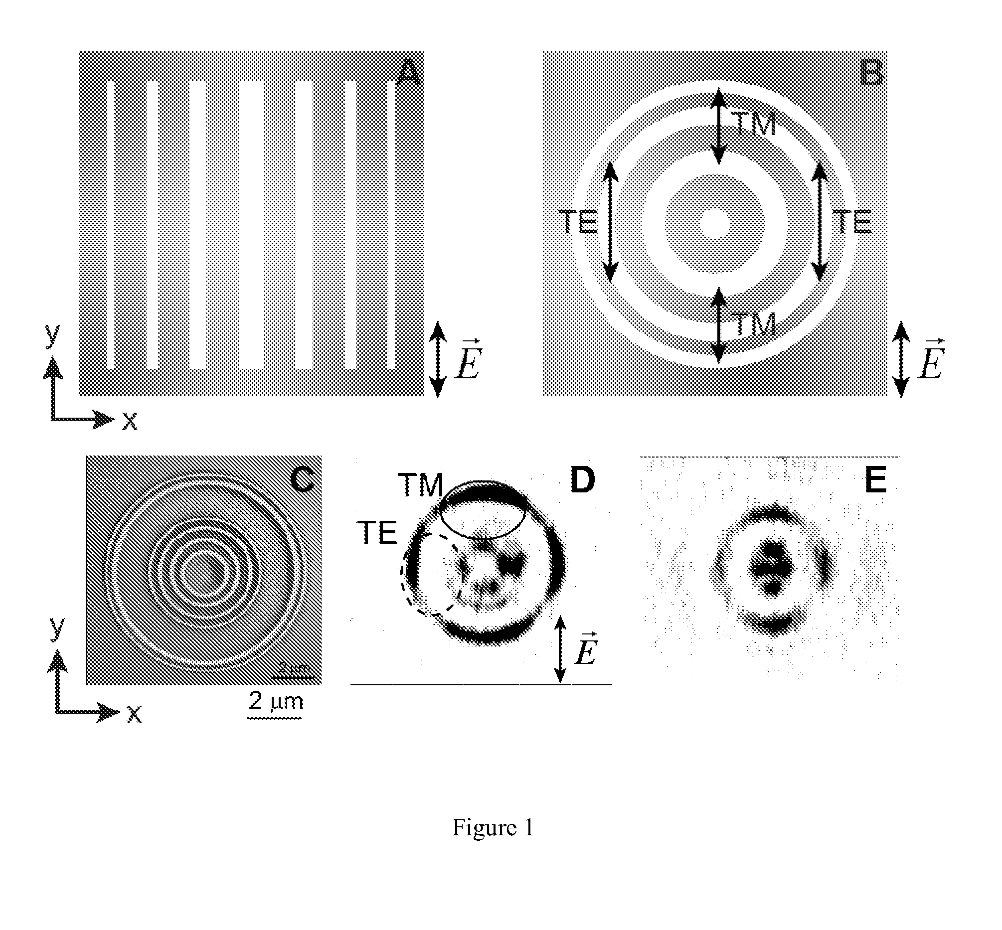
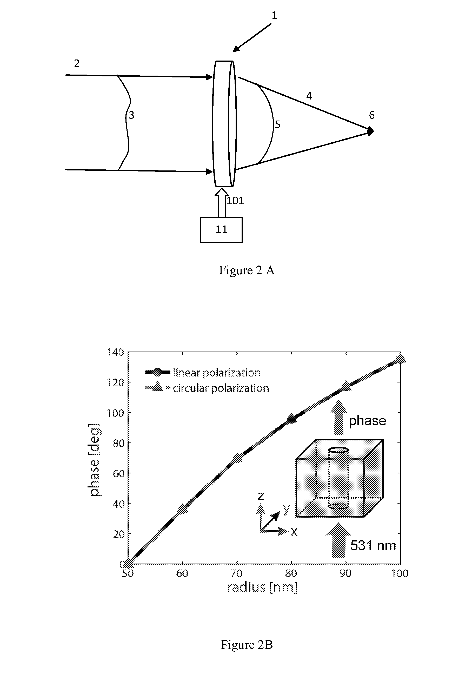
[0022]A novel optical device with nanoslits or holes is disclosed. The holes are designed in the form of straight slits (defined as holes forming a rectangular or linear shape) or non-uniform circular slits (defined as holes forming shapes such as ellipses, ovals, elongated circles, or any other non-perfect round shape). In one embodiment of the present invention, a two-dimensional traditional nanoslit arrangement (See FIG. 1A) is further developed to create a circular format. Concentric nanoslits with different widths are arranged in a pattern similar to FIG. 1B and realized, according to one embodiment of the present invention, by milling into a thin metal film. In this embodiment, the optical device will cause arbitrary waveform formation to focus linearly polarized light into a smaller circular spot. For example, when x-polarized light is transmitted through the device, some areas of the circular slit perform as slit waveguides upon TM-excitation (where the E-field is parallel t...


PUM

PropertyMeasurementUnit
focal distanceaaaaaaaaaa
refractive indexaaaaaaaaaa

Abstract

A planar optical device, comprised of sets of nanometer-scale holes milled into a thin metal or ceramic film of subwavelength thickness serves to form arbitrary waveform of light. The holes form a pattern, preferrably rings, of various sizes in order to achieve a given phase front of light due to photonic effect. When designed as a lens, the device focuses incident light into a tight focal spot. In symmetric design, the focusing property of the device does not depend on the incident polarization angle. The lens can be manufactured based on high-throughput fabrication methods and easily integrated with a chip or placed at the end of an optical fiber.

Description

CROSS-REFERENCE TO RELATED APPLICATIONS[0001]This patent application claims priority to, and incorporates fully by reference, U.S. Provisional Patent Application No. 61 / 707,939, filed Sep. 29, 2012.STATEMENT REGARDING FEDERALLY SPONSORED RESEARCH[0002]The present invention was made with governmental support under 105104, awarded by the Office of Naval Research. The government has certain rights in this invention.FIELD OF THE INVENTION[0003]This invention relates to optical devices and in particular to those devices used in compact optical systems and other micro-scale technologies.BACKGROUND OF THE INVENTION[0004]Scaling down optical elements is essential for making compact optical systems. Accordingly, planar and thin meta-structures are desirable for fabrication as well as for integration simplicity. Currently, dielectric-based refraction microlenses typically used in optical systems have a non-uniform design, with a thickness of tens of micrometers. Gradient-index lenses are plan...

Claims


Application Information

Patent Timeline
Patent Type & Authority Applications(United States)
IPC IPC(8): G02B3/08G02B1/00G02F1/365G02F1/225G02F1/39G02B3/00
CPCG02B3/08G02F1/397G02B3/0087G02F1/365G02F1/2255B82Y20/00G02F2203/06G02F2203/13G02F2203/50G02B2207/101Y10S977/888G02B1/002G02B1/005G02B5/008G02B6/1225G02B6/1226G02B6/262
Inventor KILDISHEV, ALEXANDERSATOSHI, ISHIISHALAEV, VLADIMIR
Owner PURDUE RES FOUND INC
Why Eureka
Try Eureka