

Semiconductor device and method of fabricating the same
a semiconductor and semiconductor technology, applied in the field of semiconductor devices, can solve the problems of high degree of difficulty in manufacturing such semiconductor devices, and achieve the effect of simplifying the method of fabrication
- Summary
- Abstract
- Description
- Claims
- Application Information
AI Technical Summary
Benefits of technology
Problems solved by technology
Method used
Image

Examples
first embodiment
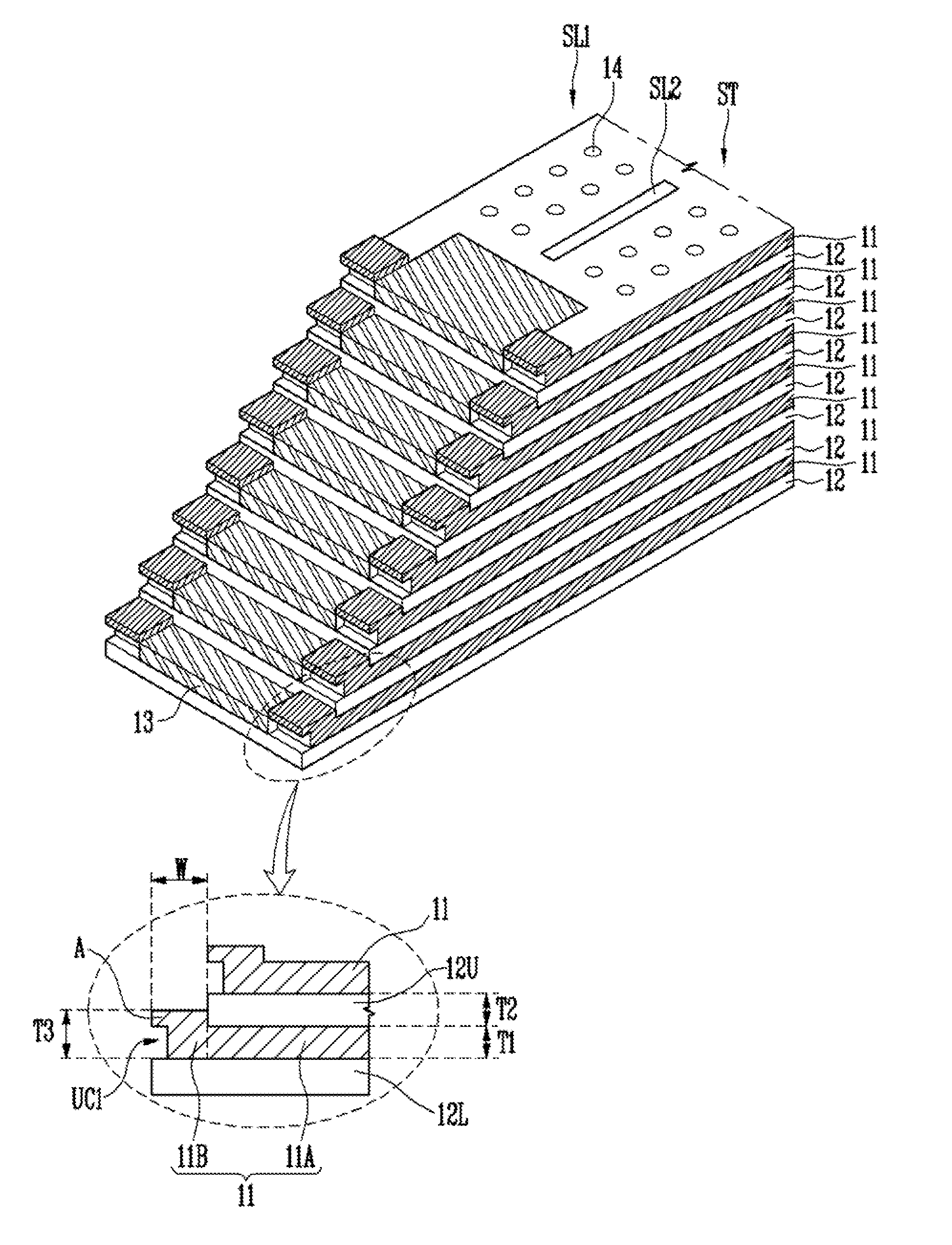
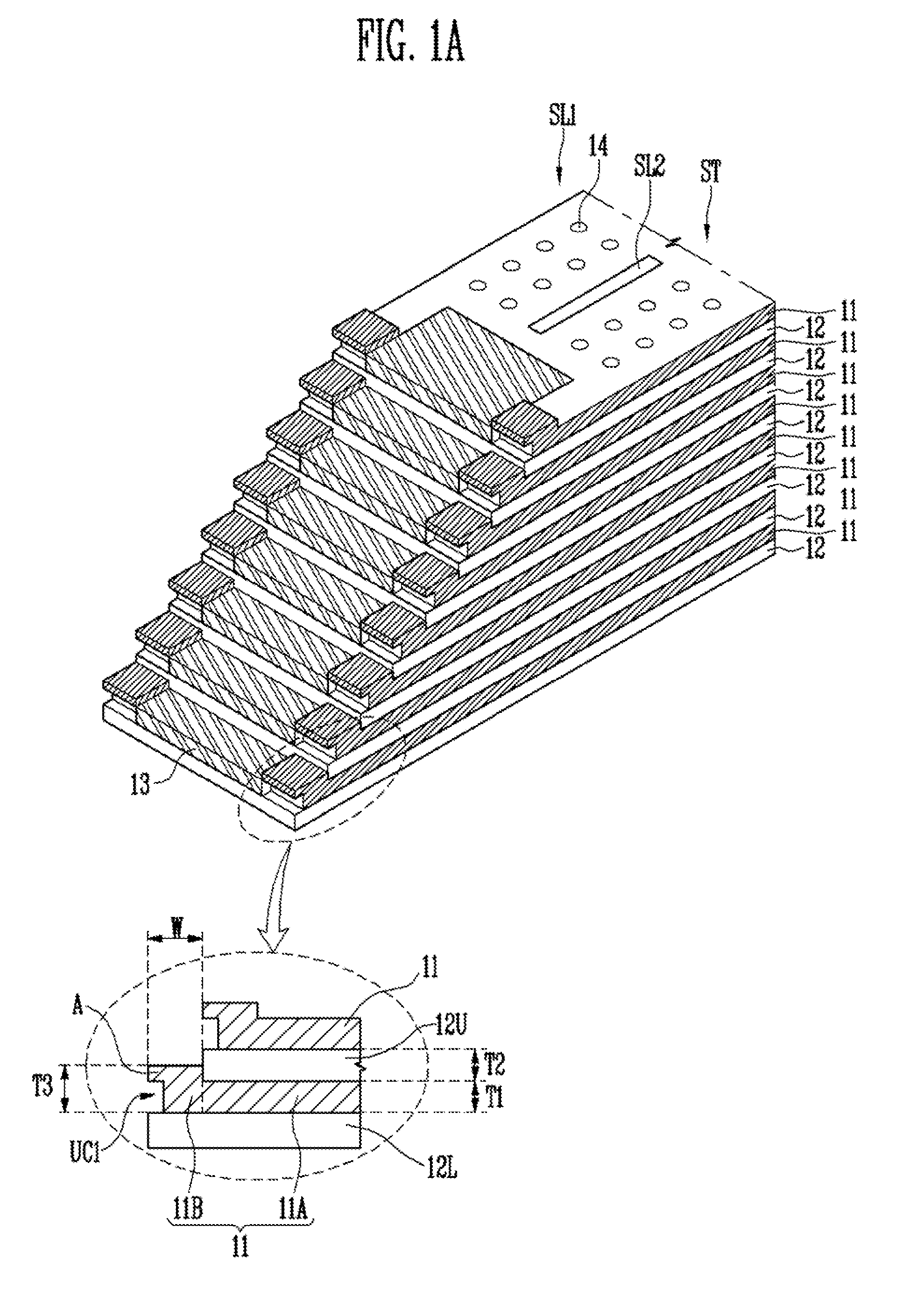
[0022]FIG. 1A is a perspective view showing a structure of a semiconductor device according to the present invention. As illustrated in FIG. 1A, the semiconductor device according to the embodiment of the present invention includes a stacked structure ST having a sidewall in the shape of stairs. The stacked structure ST includes conductive layers 11 and insulating layers 12, which are alternately stacked. For example, the insulating layers 12 are stacked in the shape of stairs, and the conductive layers 11 are interposed between the stacked insulating layers 12.
[0023]Referring to the enlarged view, each of the conductive layers 11 includes a first region 11A interposed between upper and lower insulating layers 12U and 12L, and a second region 11B protruding from between the upper insulating layer 12U and the lower insulating layer 12L. The first region 11A may be a gate electrode of a select transistor, a memory cell, etc., a word line, or a select line. Further, the second region 1...
second embodiment
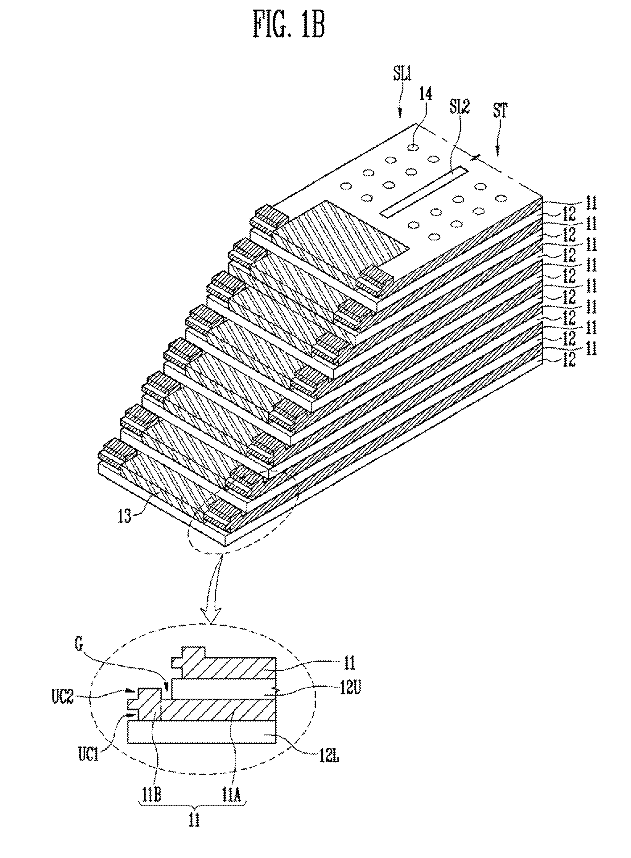
[0030]FIG. 1B is a perspective view showing a structure of a semiconductor device according to the present invention. For the sake of brevity, structures that have been previously explained will not be described again, so, for further clarity, please refer to descriptions and illustrations of previous embodiments.
[0031]As illustrated in FIG. 1B, a semiconductor device according to an embodiment of the present invention includes a stacked structure ST including conductive layers 11, insulating layers 12, sacrificial layers 13, semiconductor patterns 14, and a second slit SL2. Further, first slits SL1 are located at both sides of the stacked structure ST.
[0032]Referring to the enlarged view, each of the conductive layers 11 includes a first region 11A interposed between upper and lower insulating layers 12U and 12L, and a second region 11B protruding from between the upper insulating layer 12U and the lower insulating layer 12L. The second region 11B of each of the conductive layers 1...
third embodiment
[0034]FIG. 1C is a perspective view showing a structure of a semiconductor device according to the present invention.
[0035]As illustrated in FIG. 1C, a semiconductor device according to an embodiment of the present invention includes a stacked structure ST including conductive layers 11, insulating layers 12, sacrificial layers 13, semiconductor patterns 14, and a second slit SL2. Also, first slits SL1 are located at both sides of the stacked structure ST.
[0036]Referring to the enlarged view, each of the conductive layers 11 includes a first region 11A interposed between upper and lower insulating layers 12U and 12L and a second region 11B protruding from between the upper insulating layer 12U and the lower insulating layer 12L. The second region 11B of each of the conductive layers 11 may have a greater thickness than the first region 11A and include a first protruding part (A) formed on a sidewall of the second region 11B and a second protruding part (B) formed on an upper surface...
PUM
 Abstract
Description
Claims
Application Information