Tunnel insulation layer structures, methods of manufacturing the same, and vertical memory devices including the same

a tunnel insulation and layer structure technology, applied in semiconductor devices, semiconductor/solid-state device details, electrical apparatus, etc., can solve the problem of slow program/erase operation of vertical memory devices, and achieve the effect of preventing the loss of charge from deep trap sites

Active Publication Date: 2015-10-01
SAMSUNG ELECTRONICS CO LTD
View PDF1 Cites 14 Cited by
  • Summary
  • Abstract
  • Description
  • Claims
  • Application Information

AI Technical Summary

Benefits of technology

[0007]Example embodiments provide a tunnel insulation layer structure having an improved reliability.
[0008]Example embodiments provide a vertical memory device having an improved reliability.
[0009]Example embodiments provide a method of manufacturing a vertical memory device having an improved reliability.
[0030]According to example embodiments, the tunnel insulation layer structure may include at least four tunnel insulation layers, preferably five tunnel insulation layers, e.g., the first to fifth tunnel insulation layers. The nitrogen concentrations of the third tunnel insulation layer and the fifth tunnel insulation layer may be lower than those of the second tunnel insulation layer and the fourth tunnel insulation layer. During processes for forming the third tunnel insulation layer and the fifth tunnel insulation layer, shallow trap sites may be removed or reduced from the second tunnel insulation layer or the fourth tunnel insulation layer, so that a charge loss from deep trap sites may be prevented. Therefore, when the tunnel insulation layer structure is used in a non-volatile memory device, an initial voltage shift problem of the non-volatile memory device may be resolved or may be reduced.

Problems solved by technology

When a thickness or an equivalent oxide thickness (EOT) of the tunnel insulation layer is large, a program / erase operation of the vertical memory device may be slow.

Method used


Image

  • Tunnel insulation layer structures, methods of manufacturing the same, and vertical memory devices including the same
  • Tunnel insulation layer structures, methods of manufacturing the same, and vertical memory devices including the same
  • Tunnel insulation layer structures, methods of manufacturing the same, and vertical memory devices including the same

Examples


Embodiment Construction

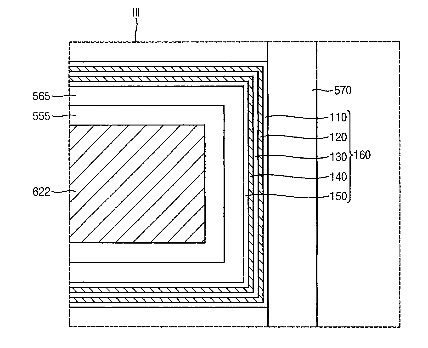
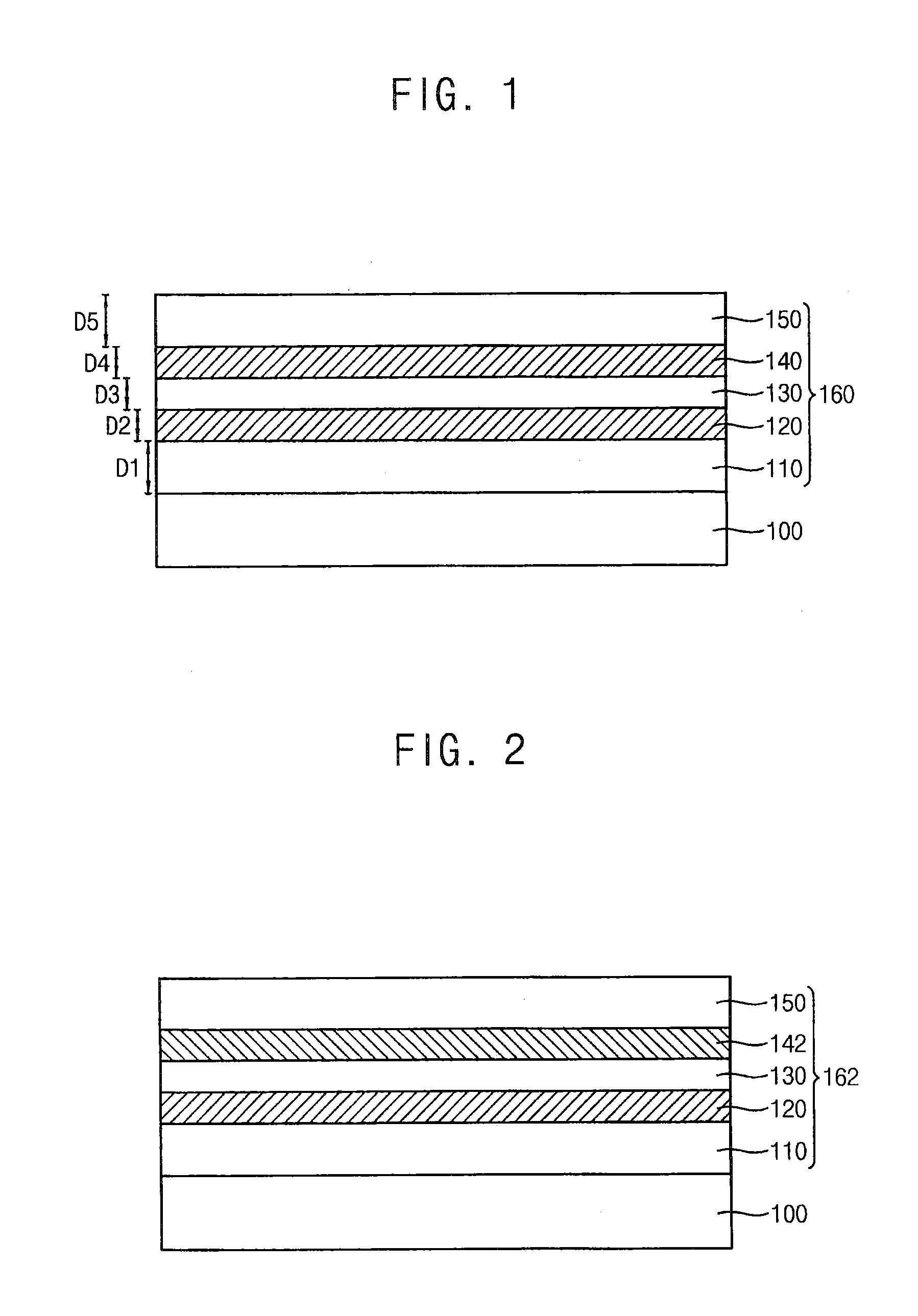
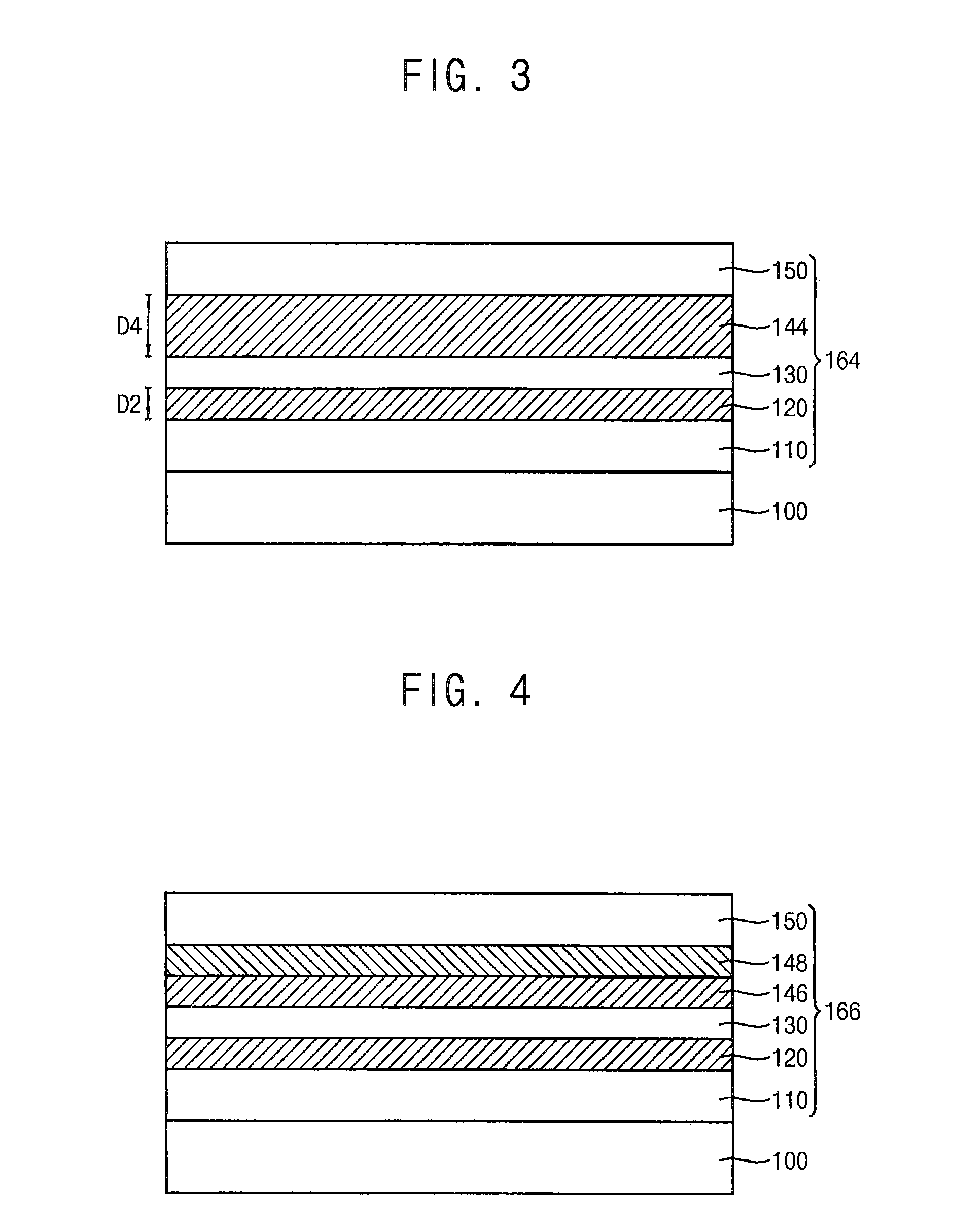
[0049]Example embodiments will now be described more fully with reference to the accompanying drawings, in which example embodiments are shown. Example embodiments may, however, be embodied in many different forms and should not be construed as limited to the example embodiments set forth herein. In the drawings, the thicknesses of layers and regions are exaggerated for clarity. Like reference numerals in the drawings denote like elements, and thus their description will be omitted.

[0050]It will be understood that when an element or layer is referred to as being “on,”“connected to” or “coupled to” another element or layer, it can be directly on, connected or coupled to the other element or layer or intervening elements or layers may be present. In contrast, when an element is referred to as being “directly on,”“directly connected to” or “directly coupled to” another element or layer, there are no intervening elements or layers present. Like numerals refer to like elements throughout...


PUM


Abstract

Tunnel insulation layer structures and methods of manufacturing the same are disclosed. The tunnel insulation layer structures may include a first tunnel insulation layer, a second tunnel insulation layer, a third tunnel insulation layer, a fourth tunnel insulation layer and a fifth tunnel insulation layer. The first tunnel insulation layer on a substrate has a first band gap energy. The second tunnel insulation layer on the first tunnel insulation layer has a second band gap energy which is lower than the first band gap energy. The third tunnel insulation layer on the second tunnel insulation layer has a third band gap energy which is higher than the second band gap energy. The fourth tunnel insulation layer on the third tunnel insulation layer has a fourth band gap energy which is lower than the third band gap energy. The fifth tunnel insulation layer on the fourth tunnel insulation layer has a fifth band gap energy which is higher than the fourth band gap energy.

Description

CROSS-REFERENCE TO RELATED APPLICATION[0001]This U.S. non-provisional application claims priority under 35 U.S.C. §119 to Korean Patent Application No. 10-2014-0037880, filed on Mar. 31, 2014, in the Korean Intellectual Property Office (KIPO), the disclosure of which is herein incorporated by reference in its entirety.BACKGROUND[0002]1. Field[0003]Example embodiments relate to a tunnel insulation layer structure, a method of manufacturing a tunnel insulation layer structure, and a vertical memory device including a tunnel insulation layer structure. More particularly, example embodiments relate to a vertical memory device having a vertical channel and including the tunnel insulation layer structure.[0004]2. Description of the Related Art[0005]In methods of manufacturing vertical memory devices, an insulation layer and a sacrificial layer may be alternately and repeatedly formed on a substrate. Holes may be formed through the insulation layers and the sacrificial layers. Channels may...

Claims


Application Information

Patent Timeline
Patent Type & Authority Applications(United States)
IPC IPC(8): H01L29/51H01L21/28H01L27/115
CPCH01L29/513H01L21/28282H01L27/11582H01L29/518H01L29/40117H10B43/27H10B41/48
Inventor CHOI, EUN-YEOUNGNOH, YOUNG-JINKIM, BI-OPARK, KWANG-MINAHN, JAE-YOUNGYUN, JU-MICHOI, JAE-HOHWANG, KI-HYUN
Owner SAMSUNG ELECTRONICS CO LTD
Why Eureka
Try Eureka