Light emitting element and light emitting device using the same

a technology of light emitting devices and light emitting elements, which is applied in the direction of basic electric elements, electrical devices, and semiconductor devices, can solve problems such as deviations in luminance distribution, and achieve the effect of reducing uneven luminance distribution

Active Publication Date: 2015-10-01
NICHIA CORP
View PDF2 Cites 32 Cited by
  • Summary
  • Abstract
  • Description
  • Claims
  • Application Information

AI Technical Summary

Benefits of technology

[0009]According to an embodiment, a light emitting element with reduced uneven l

Problems solved by technology

The inventors conducted vigorous studies on the shapes and the arrangements of the n-side electrode and the p-side electrode in a light emitting element and have found that even when the regions (hereinafter may be referred to as “ex

Method used


Image

  • Light emitting element and light emitting device using the same
  • Light emitting element and light emitting device using the same
  • Light emitting element and light emitting device using the same

Examples


embodiment 1

Light Emitting Element

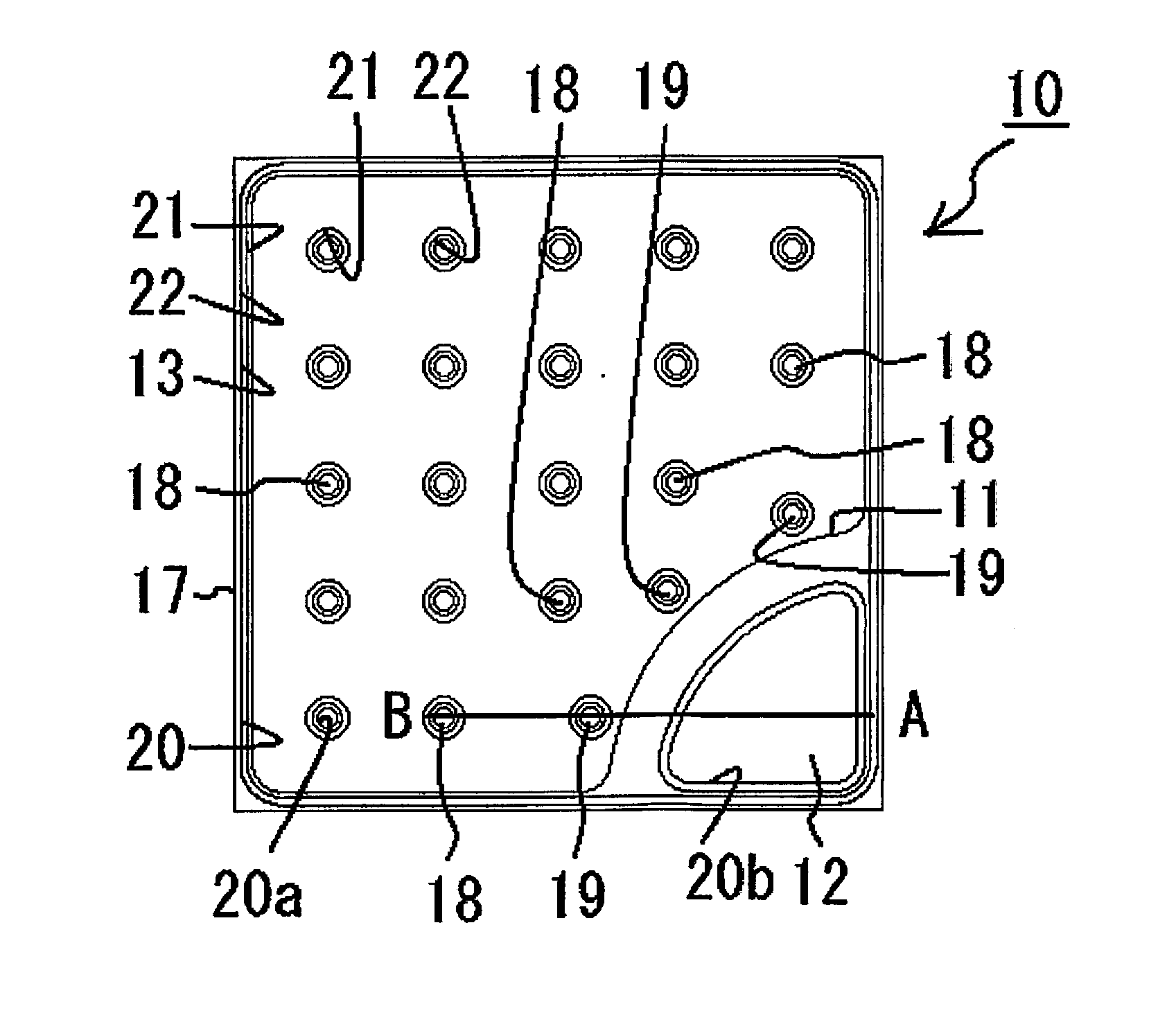
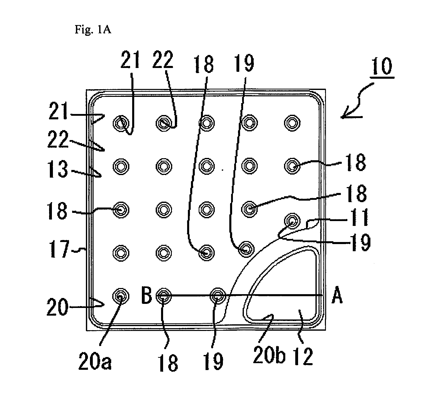
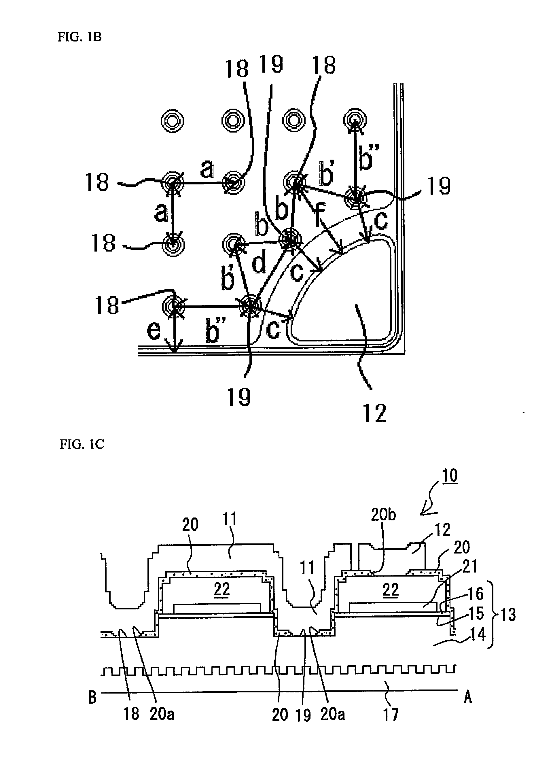
[0066]The light emitting element 10 according to Embodiment 1 includes, as shown in FIG. 1A to FIG. 1D, a semiconductor stacked layer body 13 having an approximately square shape in a plan view, an n-side electrode 11 and a p-side electrode 12 respectively connected to corresponding portions on a same surface side of the semiconductor stacked layer body 13. The length of one side of the light emitting element 10 is 1.4 mm.

[0067]The semiconductor stacked layer body 13 is constituted with an n-type semiconductor layer 14, an active layer 15, and a p-type semiconductor layer 16 disposed in this order on a sapphire substrate which has an approximately square shape in a plan view with a protrusion-recess shape on its upper surface.

[0068]The semiconductor stacked layer body 13 has a plurality of exposed portions on its inward side, where portions of the p-type semiconductor layer 16 and the active layer 15 are removed to expose corresponding portions of the n-type se...

embodiment 2

Light Emitting Element

[0077]The light emitting element 40 according to Embodiment 2 includes, as shown in FIG. 1A to FIG. 1D, a semiconductor stacked layer body 13 having an approximately square shape in a plan view, an n-side electrode 51 and a p-side electrode 52 respectively connected to corresponding portions on a same surface side of the semiconductor stacked layer body 13. The configurations of the sapphire substrate 17 and the semiconductor stacked layer body 13 are similar to the configuration of the light emitting element 10. The first exposed portions 18 and the second exposed portion 19 are, in a plan view, arranged in a similar manner as in the light emitting element 10 of Embodiment 1.

[0078]A light-transmissive electrically conductive layer 53 (a thickness of about 0.1 μm) of an ITO is disposed on approximately the entire surfaces of the first exposed portions 18 and the second exposed portions 19 and on approximately the entire upper surface of the p-type semiconductor...

embodiment 3

Light Emitting Device

[0090]As shown in FIGS. 4A to 4C, the light emitting device 60 includes the light emitting element 10 according to Embodiment 1, and a base member 61 which has a wiring pattern on its surface. The wiring pattern includes a pair of patterns being a positive pattern and a negative pattern. Preferably, auxiliary patterns further connect the positive pattern and the negative pattern.

[0091]In order to mount a light emitting element in a face-down manner, the n-side electrode 11 and the p-side electrode 12 of the light emitting element 10 are respectively connected to the corresponding wiring patterns of the base member 61 via a joining member. In this case, the joining member may be disposed not at the light emitting element 10 side but at the wiring pattern side of the base member 61.

[0092]In the light emitting device 60, the light emitting element 10 is covered with the light-transmissive member 63. The sealing member 63 is, for example, made of a silicone resin co...


PUM


Abstract

A light emitting element includes a semiconductor stacked layer body having an n-type semiconductor layer, an active layer, and a p-type semiconductor layer in this order, and a plurality of exposed portions defined at an upper surface side of the semiconductor stacked layer body, the plurality of exposed portions respectively exposing a part of the n-type semiconductor layer, a p-side electrode arranged in a first region and electrically connected with an upper surface of the p-type semiconductor layer and, arranged at one corner above the p-type semiconductor layer in a plan view, and an n-side electrode electrically integrally connected to the plurality of exposed portions and arranged in a different region in a plan view. In a plan view, the semiconductor stacked layer body has a rectangular shape and the plurality of exposed portions includes, a plurality of first exposed portions arranged at substantially equal intervals along a side of the semiconductor stacked layer body and a plurality of second exposed portions arranged closer to the p-side electrode than the first exposed portions are to the p-side electrode. The plurality of second exposed portions include at least one second exposed portion which has a shortest distance to the first exposed portions, the shortest distance to the first exposed portions being longer than a shortest distance among the first exposed portions. The at least one second exposed portion also has a shortest distance to the p-side electrode shorter than the shortest distance among the first exposed portions.

Description

CROSS-REFERENCE TO RELATED APPLICATION[0001]This application claims priority to Japanese Patent Application No. 2014-069816, filed on Mar. 28, 2014. The entire disclosure of Japanese Patent Application No. 2014-069816 is hereby incorporated herein by reference.BACKGROUND[0002]1. Technical Field[0003]The present disclosure relates to a light emitting element and a light emitting device using the light emitting element.[0004]2. Background Art[0005]In order to obtain good light extraction efficiency and uniform emission in light emitting elements, various researches have been conducted on the shapes and arrangements of n-side electrodes and p-side electrodes. For example, in US 2011-0127568A1, a configuration is proposed, in which a plurality of circular regions for connecting the n-electrode to the semiconductor layer are arranged evenly in the entire light emitting region and the p-electrode is located at a side of the light emitting element.SUMMARY OF THE INVENTION[0006]It is an asp...

Claims


Application Information

Patent Timeline
IPC IPC(8): H01L33/38H01L33/52H01L33/62
CPCH01L33/38H01L33/52H01L33/62H01L33/382H01L33/387H01L33/40H01L33/44H01L33/54
Inventor TAKENAGA, KOICHIKAWAGUCHI, HIROFUMIKASHIMOTO, KAZUKI
Owner NICHIA CORP
Why Eureka
Try Eureka