[0026]It is the objective of the current invention to: a) provide a method to fabricate one or multiple self-aligned gate aperture around a single or a small cluster of CNT and with equal distance to each CNT; b) provide a method for controlling CNT growth over large area so that they are either mono-dispersed or dispersed in small clusters, with a narrow distribution in CNT
diameter and the number of CNT in each cluster, and, furthermore, the spacing between the single or cluster of CNT is large enough to enable a gate aperture around each one of them and yet small enough in order that the emitter density can be as high as 108 / cm2; and c) provide a means for enabling favorable
wide band gap
semiconductor nano-structures to be utilized as field emitters.
[0027]It is another object of the invention to provide an
electron source using a single or a small cluster of dispersed nano-structures that: a) has emission properties which can be modulated with a
low voltage, b) has a high emission site density, c) emits uniformly over large area, d) generate a highly collimated electron beam, e) has
high energy efficiency, f) is robust to
ion bombardment and
chemical attack, and g) is easy to fabricate with high production yield.
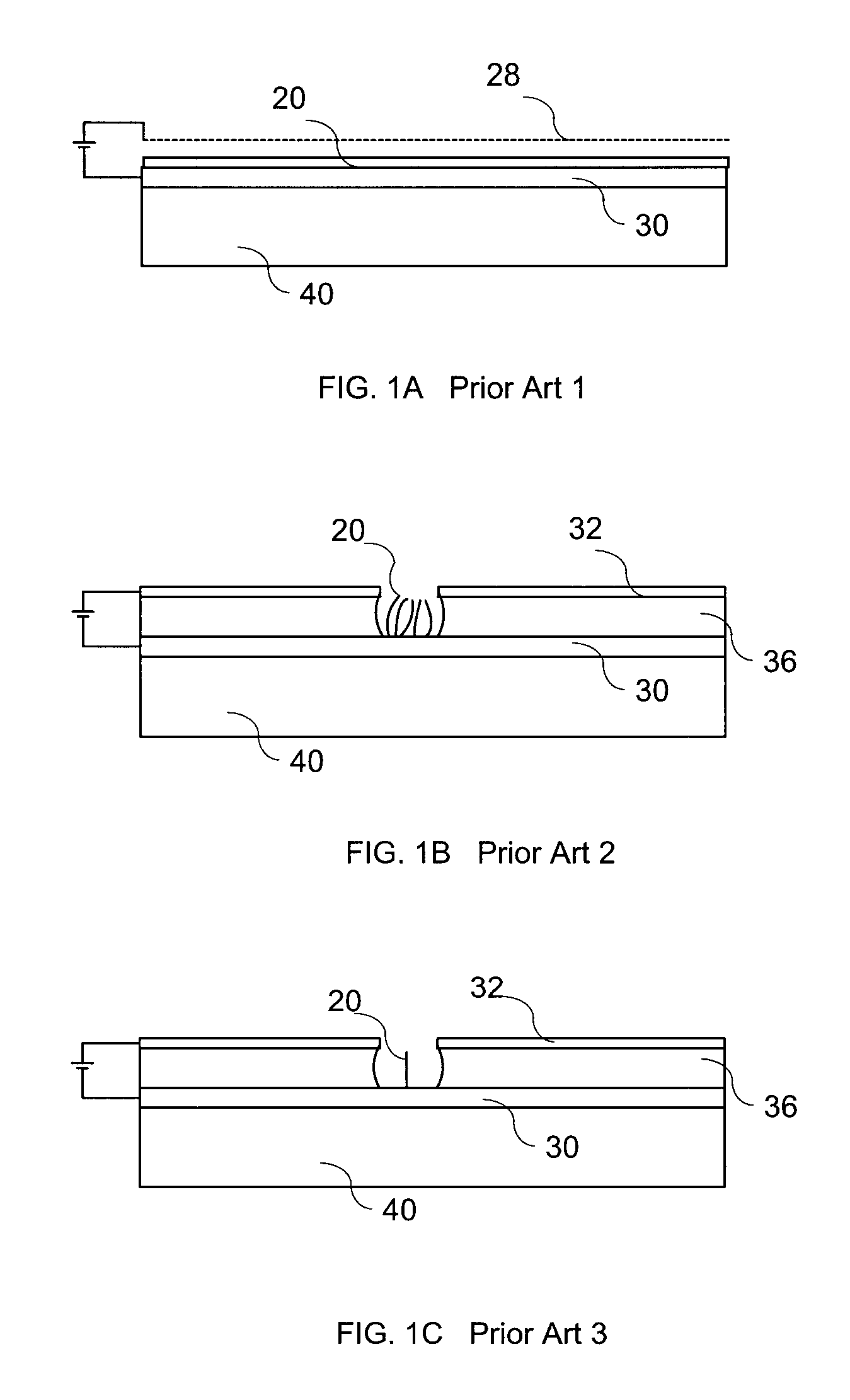
[0031]Self-alignment of an aperture, as is described in the current invention, means the location where the incline CNT is grown or assembled can be random and needs not be predetermined. The spacing between CNTs, in this invention, may be as low as one
micrometer or less. Therefore, two orders of magnitude higher emitter density over prior art is possible and advantages can be taken of CNT growth or
assembly controlling processes that don't require expensive and complicated
lithography.
[0032]One of such enabled embodiments is to use an
ion-track-etched membrane as a
hard mask for patterning catalyst before CNT growth. Preferred membranes are those with a pore density between 1×10⁵ to 1×10⁹ pores / cm2 and pore sizes from 10 nm to a few micrometers. It is known that for CNT growth, its
diameter and the inter-tube spacing are determined by those of catalyst. When the catalyst size is less than 200 nm, a single CNT is likely grow from each particles. When membrane with larger pores is used, a small cluster of CNT, 3 to 5 for instance, can grow from each particle. Catalyst deposition through an
ion-track-etched membrane with chosen pore size and density will produce an array of catalyst particles with substantially
uniform size and desirable average inter-tube or inter-cluster spacing.
[0033]The advantages of using the ion-track-etched membranes as a
shadow mask for catalyst deposition include: a) pore size and density are in the most desirable range and are highly controlled, b) inexpensive, widely available, and come in sizes particularly suitable for large
flat panel display applications, and c) it is easy to apply them to a
substrate surface as a
shadow mask and they can be recycled in production, provided the catalyst is removed after each deposition. Both the substrate and the membrane can be surface treated so that they attract to each other, resulting a smooth and uniform
overlay on the substrate.
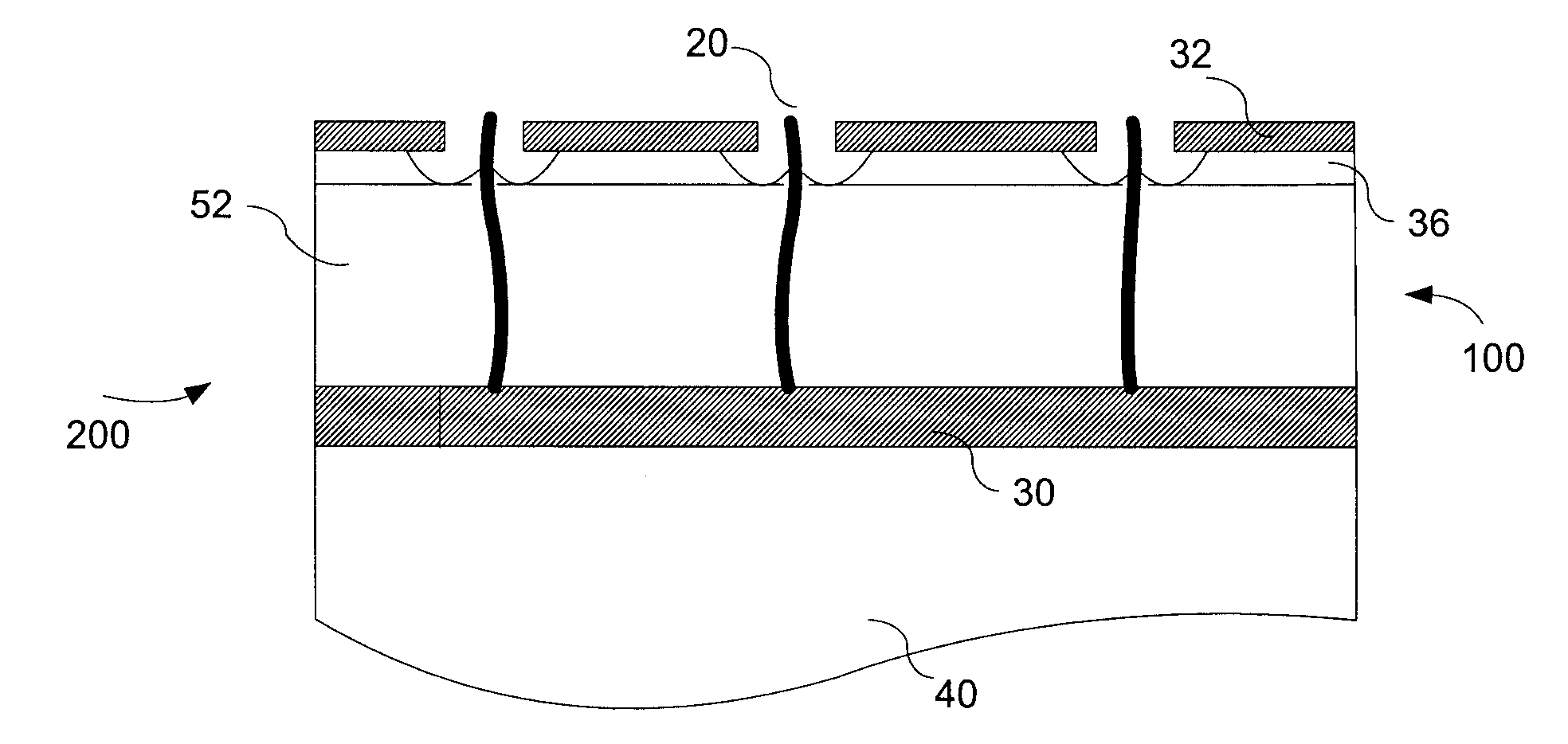
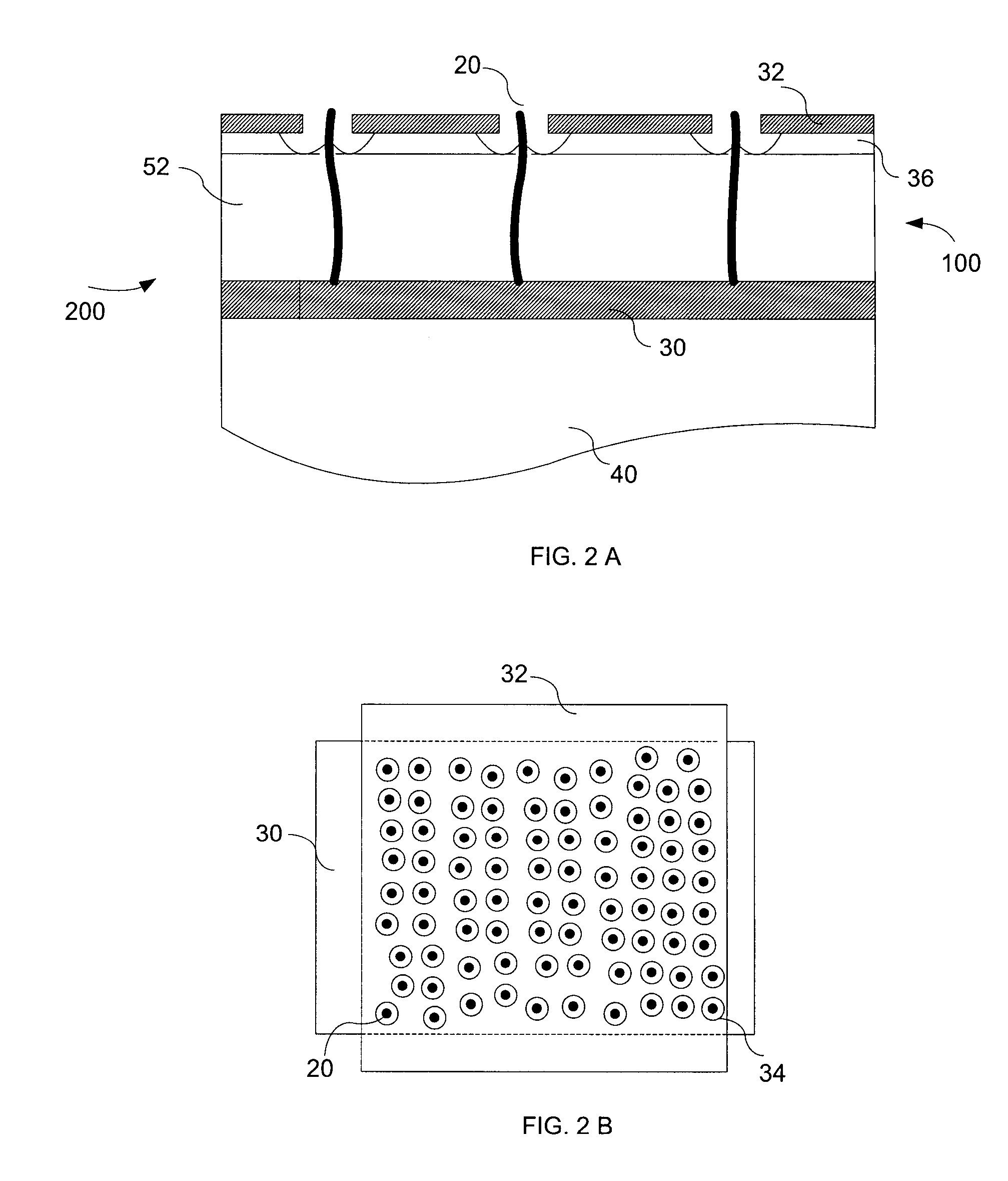
[0039]In accordance with the current invention, the emitter, whether it is a single nano-structure or a small cluster of nano-structures, will always perfectly located at the center of the aperture regardless its location, and size, and the distance between the aperture and emitter (the emitter-to-gate distance d) is substantially the same over the entire
substrate surface, on the order of 100 nm, and controllable by the thickness of the
gate insulator. And, all the emitters have substantially the same length and
diameter. A gated field emission
electron source with these characteristics provides an
extra low voltage modulation, uniform emission over large area, and low
energy loss from
gate current. Since the emitter is largely embedded in a
dielectric, it is mechanically and chemically protected and, to some extent, shielded from
ion bombardment, giving rise to a longer lifetime and steadier electron emission. With a proper selection, the embedding material can also enhance the
thermal conduction from the emitter. When a
dielectric is used as the embedding material, the relatively large gap between the
cathode and the gate electrodes also reduces the occurrence of a short circuit between them and the capacitive
energy consumption during the emission modulation, resulting in a higher production yield and higher energy efficiency. An array of emitters with a density as high as 1 / cm2 will produce a more homogeneous emission compared to those of low emitter density.

